APP

Chipsmith

STEP-native chip validator β€” 5-source cross-validation, OCCT-generated copyright-free 3D models with embedded signal annotations, datasheet-to-STEP pipeline.

Chipsmith
πŸ’¬ Sample prompts Paste any of these into Claude Code to use this app
Open library Open chipsmith for VL53L8CX
Detect Run detection on LM358D
Sign off Sign off this chip and bake the STEP
Place pin-1 Place a pin-1 dimple on the NE corner
Heatsink Show heatsink vias under the EP
Cross-validate Compare all 5 footprint sources
Generate chip Show the Adom-generated 3D chip from the datasheet
Faux PCB Show the 1.6mm faux PCB with drill holes
⚑ Install this app

Paste this into Claude Code (VS Code panel, Adom editor, or terminal) to install:

I want to install the "Chipsmith" app from the Adom Wiki (https://wiki-ufypy5dpx93o.adom.cloud/wiki/apps/adom-chipsmith). For the Docker CLI: curl -fsSL https://wiki-ufypy5dpx93o.adom.cloud/static/apps/adom-chipsmith/adom-chipsmith -o /usr/local/bin/adom-chipsmith && chmod +x /usr/local/bin/adom-chipsmith && adom-chipsmith install Then verify the install works.

Download latest

⊞ Windows coming soon
macOS coming soon
🐧 Linux coming soon
🐳 Adom Docker CLI adom-chipsmith ·

See all releases on GitHub (private repo β€” access required)

adom-chipsmith β€” STEP-native chip validator

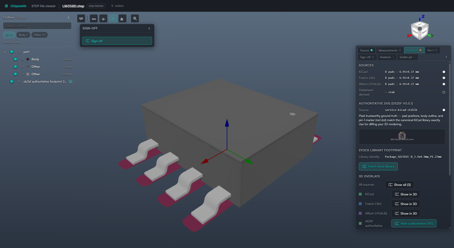
adom-chipsmith loads a chip's STEP file alongside its footprint, datasheet PDF, and a chipsmith-spec manifest, then runs detection on the STEP B-rep (not on triangulated GLB meshes), validates measurements, layers a 1.6 mm faux PCB, auto-generates heatsink-via grids under any exposed pad, lays out solder-jet domes per the solder-jetting rules, and on user sign-off bakes a canonical <mpn>.chipsmith.step plus a sidecar JSON for downstream Adom tools.

It's the higher-level validator that sits on top of adom-step β€” chipsmith inherits the canonical Babylon viewer + smart-pick measure tool + Outline pane via the Tier-3 importer pattern from 3d-viewer-design Β§2.

What it does (in one screen)

TabWhat it shows
SourceManifest (MPN / mfr / package), declared spec (pin_count / structural_type / body_dims_mm), file paths with reveal-in-VSCode buttons, datasheet via adom-pdf-viewer. Inline editor saves into info.json.
MeasurementsAuto-rescale negotiation across 6 candidates (Γ—1, Γ·25.4, Γ·1000, Γ—25.4, Γ—1000, Γ·10) β€” picks the scale within Β±5% of declared body_dims_mm. mm + mils dual readout.
DetectionMode 0 walks the named scene graph. Mode 1 falls back to surface-type clustering on /api/step-meta. Pin-reveal strobe flashes each detected feature with a numbered HTML badge floating at the screen-projected XY.
FootprintPer-source breakdown across KiCad / Fusion / Altium / datasheet-derived. Cross-source agreement matrix (pad-by-pad position + size deltas). 3D toggle per source β€” translucent pads at z=0 in the scene. ds2sf v0.5.1 authoritative SVG rendered as real vector polygons via earcut (not a raster texture; sharp at any zoom).
Pin-1Chip-side via Mode 0 detection; footprint-side via silkscreen marker scan. Place-synthetic-indicator UI (NW/NE/SW/SE/click) when chip-side is missing. Three shapes: dimple / raised dot / corner chamfer.
Sign-off4 hard + 3 soft gates. CTA POSTs to /api/signoff β†’ writes <mpn>.chipsmith.json + bakes <mpn>.chipsmith.step.
HeatsinkEP detection + auto-generated 0.3 mm via grid (1.2 mm pitch, 0.4 mm margin). Hollow plated barrels with copper annular rings. CSG-drilled B.Cu copper pour underneath the EP β€” with via-clearance holes β€” for the heatsink path.
Solder-jet300 Β΅m dome layout per solder-jetting β€” intra-pad β‰₯100 Β΅m, inter-pad β‰₯300 Β΅m with no-bridging pruning.

Every overlay layer is a first-class Outline citizen with eye-toggle, click-to-isolate, and a right-click menu.

STEP-native, not GLB

Both adom-chipfit and adom-chiplinter operate on triangulated GLBs and both lose surface-type information (a BGA ball becomes a triangle list, indistinguishable from a QFN pad). chipsmith reads the STEP file's B-rep + assembly hierarchy directly via service-step2glb's /step-meta endpoint, so:

  • CYLINDER + small radius + dome top β†’ BGA ball.
  • PLANE + horizontal + at zβ‰ˆseat-plane β†’ SMD pad.
  • PLANE + vertical + tall (β‰₯1.6 mm) + thin β†’ through-hole pin.
  • CONICAL or CYLINDER on top, small radius, elevated β†’ pin-1 indicator candidate.

Detection runs in three modes β€” Mode 0 named-scene-graph walk, Mode 1 surface-type cluster, Mode 2 face-merge fallback β€” stopping when β‰₯(declared pin count) features have been classified.

Multi-source footprint cross-validation

chipsmith renders four parallel footprint sources from chip-fetcher's library (datasheet-derived, KiCad, Fusion 360 .lbr, Altium .PcbLib) into the scene as separately-branched overlays in different tints (orange / green / blue / purple), then runs a per-pad cross-validation matrix. All four sources agreeing pad-by-pad is the strongest possible "chipsmith nailed this chip" signal β€” disagreements pop visually and gate sign-off.

The ds2sf authoritative SVG (when present in the chip-fetcher library β€” emitted by ds2sf v0.5.1+) renders as a fifth branch of pixel-trustworthy ground truth: real vector polygons parsed from the SVG and triangulated via earcut, not a texture-mapped raster.

Quick start

# Install (paste into Claude Code):
curl -fsSL https://wiki-ufypy5dpx93o.adom.cloud/static/apps/adom-chipsmith/adom-chipsmith \
  -o /usr/local/bin/adom-chipsmith && chmod +x /usr/local/bin/adom-chipsmith && \
  adom-chipsmith install

# Open a chip from a chip-fetcher library
adom-chipsmith view-library /home/adom/project/chip-fetcher/library/VL53L8CX

# Open an arbitrary STEP + footprint + datasheet
adom-chipsmith view path/to/chip.step \
  --footprint path/to/chip.kicad_mod \
  --spec      path/to/info.json

# Headless detection β€” JSON report
adom-chipsmith detect --json /path/to/chip-fetcher/library/<MPN>

CLI surface

CommandPurpose
view <step> [--footprint] [--spec] [--datasheet] [--no-open]Open one chip
view-library <chip-fetcher-dir>Open a chip from a chip-fetcher library
start --port N / stop --port N / status / healthServer lifecycle
list-componentsScene-graph component tree
isolate <name> / show <name> / hide <name> / show-all / frame <name>Visibility + camera
place-pin1 <corner> / set-overlay <kind> <on/off> / sign-offVerification flow drivers
screenshot --out <png>PNG of current canvas
eval <js>Run a JS expression inside the webview, print the result
console -fTail JS console output from the webview
detect --jsonHeadless detection report on a chip-fetcher dir

JS API surface (window.adomChipsmith)

The full UI is JS-shadowed for AI demo scripts + tests. From the CLI: adom-chipsmith eval "window.adomChipsmith.<verb>(...)".

state()                         // full state snapshot
setActiveTab(id)                // 'source' | 'measurements' | … | 'solderjet'
runDetection()                  // re-fetch + re-run Mode 0 β†’ Mode 1 fallback
runMeasurements()               // re-run rescale negotiation
recomputeStatuses()             // refresh every status pill from current state

placePin1(opts)                 // {mode:'corner'|'fpMarker'|'click', corner, xyMm, shape}
removePin1User()

setFootprintOverlay(src, on)    // 'kicad' | 'fusion' | 'altium' | 'datasheet' | 'stock'
setDs2sfVisible(on)
setFauxPcbVisible(on)
setHeatsinkVisible(on)
setSolderJetVisible(on)

replayReveal()                  // re-runs the strobe + numbered badges
hoverAt({x, y})                 // returns same payload as the visible HUD

signoff.gates()
signoff.canSignOff()
signoff.signOff()               // POST /api/signoff β†’ writes JSON + bakes STEP

Sign-off artifacts

FileContent
<mpn>.chipsmith.jsonFull state β€” applied scale, detected breakdown, heatsink grid, solder-jet layout, pin-1 user-placed corner, sign-off timestamp
<mpn>.chipsmith.stepCanonical role-tagged STEP via service-step2glb's /bake endpoint. Future Adom tools should prefer this over the original input.

Source

adom-inc/adom-chipsmith (private). The wiki carries the binary + SKILL.md + this page; the public install path is fully self-service.

Adjacent skills

ADOM
adom-chipsmith 19 days ago
v0.2.0 β€” proper outline names for OCCT-generated products
v0.2.0 fix: outline names show signal names (1 (OUT1)) instead of XCAF label paths (=>[0:1:1:N])John Lauer Β· 19 days ago
9.7 MB

Install notes

Adom Docker CLI install steps
curl -fsSL https://wiki-ufypy5dpx93o.adom.cloud/static/apps/adom-chipsmith/adom-chipsmith -o /usr/local/bin/adom-chipsmith && chmod +x /usr/local/bin/adom-chipsmith && adom-chipsmith install

AI Skill β€” how Claude uses this app

Edit AI Skill

name: adom-chipsmith description: > STEP-native chip detection + footprint validation + sign-off β€” the higher-level validator on top of adom-step. Loads a .step + footprint + datasheet PDF + chipsmith-spec manifest, reads B-rep + assembly hierarchy directly (NOT GLB triangle meshes), detects every electrical-contact feature (legs / pads / balls / tabs / EP / through-hole pins / reinforcement tabs) via Mode 0 (named scene- graph walk) with Mode 1 (surface-type clustering) fallback, validates measurements against declared body_dims_mm with mm-vs-m-vs-inch auto-rescale, detects pin-1 chip-side AND footprint-side, layers a 1.6mm faux PCB plate, auto-generates 0.3mm heatsink-via grid under any EP, lays out 300Β΅m solder-jet domes per the solder-jetting skill, optionally lets the user place a synthetic pin-1 indicator, and on sign-off bakes a <mpn>.chipsmith.step (canonical) + sidecar JSON. Every overlay layer is a first-class Outline citizen with eye-toggle / click-to-isolate / right-click menu. Trigger words β€” chipsmith, chip detection, validate chip step, sign off chip, footprint validation, pin-1 indicator, place pin1, heatsink vias, faux pcb, solder jet domes, manual orient step, mm vs inch step, detect pins step, chip pad detection, chip step bake, role tag chip, multi-source footprint cross-validation.

adom-chipsmith β€” STEP-native chip validator

Higher-level validator on top of adom-step. Loads a chip's STEP file alongside its footprint + datasheet + manifest, runs detection on the STEP B-rep (not the GLB triangle mesh), validates measurements, detects pin-1, layers a 1.6mm faux PCB + heatsink vias + solder-jet domes, and on user sign-off bakes a <mpn>.chipsmith.step + sidecar JSON.

Architecture: Tier-3 importer per 3d-viewer-design Β§2 β€” chipsmith inherits adom-step + the canonical Babylon viewer via git submodule chain. Upstream fixes flow β†’ adom-step β†’ chipsmith automatically.

Quick start

# Open a chip from a chip-fetcher library
adom-chipsmith view-library /home/adom/project/chip-fetcher/library/VL53L8CX

# Open an arbitrary STEP + footprint + datasheet
adom-chipsmith view path/to/chip.step --footprint path/to/chip.kicad_mod --spec path/to/spec.json

# Print the chip's scene-graph
adom-chipsmith list-components

# Headless detection β€” JSON report
adom-chipsmith detect --json

Verification surface β€” pup, not Hydrogen webview

Visual verification of chipsmith always happens in a pup window (Chrome via adom-desktop browser_*), not a Hydrogen webview tab. The chipsmith UI is multi-pane (outline left, canvas center, 7-tab sidebar right, floating sign-off HUD top-right) and gets cramped in a half-Hydrogen pane next to VS Code; pup gives it a dedicated window. (chipfit / aci use Hydrogen β€” chipsmith does not.)

# Always check existing pup sessions BEFORE opening β€” see pup skill,
# "Cross-sessionId duplicates" section. After a conversation compaction
# a prior session's chipsmith window may still be alive under a stale
# sessionId, so spawning a new one creates a duplicate.
adom-desktop browser_status '{}'

# When opening for the first time
adom-desktop browser_open_window '{"sessionId":"chipsmith","profile":"chipsmith","url":"https://chipsmith-<slug>.adom.cloud/"}'
adom-desktop browser_focus_window '{"sessionId":"chipsmith"}'

Public proxy registration: chipsmith binds 0.0.0.0:8872 (so cloudflared can reach it through the container bridge), then adom-cli carbon containers port-add --port 8872 --prefix chipsmith <slug> exposes it as chipsmith-<slug>.adom.cloud. Loopback-only binds will get HTTP 502 from the public URL even though local curl returns 200.

What the 8 tabs do

TabWhat it showsStatus pill semantics
SourceManifest (MPN / mfr / package), declared spec (pin_count / structural_type / body_dims_mm), file paths with reveal-in-VSCode buttons, datasheet via adom-pdf-viewer. Inline editor for spec fields β€” saves into info.json.● when all 3 spec fields present, ◐ partial, β—‹ none
MeasurementsAuto-rescale negotiation across 6 candidates (Γ—1, Γ·25.4, Γ·1000, Γ—25.4, Γ—1000, Γ·10) β€” picks the scale within Β±5% of declared body_dims_mm. mm + mils dual readout.● if Γ—1, ◐ if non-1 rescale, βœ— if no scale fits
DetectionMode 0 walks the named scene graph; Mode 1 falls back to surface-type clustering on /api/step-meta when Mode 0 finds <70%. Click-to-isolate per feature. Pin-reveal strobe flashes each detected feature with a numbered HTML badge floating at the screen-projected XY.Coverage-based: ●/◐/βœ—
FootprintPer-source breakdown across KiCad / Fusion / Altium / datasheet-derived. Cross-source agreement matrix (pad-by-pad position + size deltas). 3D toggle per source β€” translucent pads at z=0 in the scene.●/◐ based on sources present
Pin-1Chip-side via Mode 0 detection; footprint-side via silkscreen marker scan. Place-synthetic-indicator UI (NW/NE/SW/SE buttons) when chip-side missing.●/◐/βœ— based on agreement
Sign-offGate evaluator. 4 hard + 3 soft gates. CTA POSTs to /api/signoff β†’ writes <mpn>.chipsmith.json + bakes <mpn>.chipsmith.step.● when all hard gates pass
HeatsinkEP detection + auto-generated 0.3mm via grid (1.2mm pitch, 0.4mm margin). 3D toggle renders Cu-tone plated bores + annular pads.● if EP found, ─ N/A otherwise
Solder-jet300Β΅m dome layout per solder-jetting β€” intra-pad β‰₯100Β΅m, inter-pad β‰₯300Β΅m with no-bridging pruning. 3D toggle renders half-spheres on each pad.● when domes generated

Right-pane HUD shape

The 8-tab pane is a floating draggable HUD, not a docked column. Drag the tab strip to reposition; position persists in localStorage. P toggles collapse, 1-8 jump to tabs. Default landing at top:170, right:10 so the HUD never covers the ViewCube top-right.

Outline integration (load-bearing rule)

Every 3D overlay chipsmith adds β€” footprint pads (per source), 1.6mm faux PCB plate, heatsink vias, solder-jet domes, user-placed pin-1 indicator β€” appears as a first-class entry in the left-side Outline, with eye-toggle, click- to-isolate, right-click menu, search visibility. Per 3d-viewer-design Β§14.

CLI surface

CommandPurpose
view <step> [--footprint <kicad_mod>] [--spec <json>] [--datasheet <pdf>] [--no-open]Open one chip
view-library <chip-fetcher-dir>Open a chip from a chip-fetcher library
start --port N / stop --port N / status / healthServer lifecycle
list-componentsScene-graph component tree
isolate <name> / show <name> / hide <name> / show-all / frame <name>Visibility + camera
screenshot --out <png>PNG of current canvas
eval <js>Run a JS expression inside the webview, print the result
console -fTail JS console output from the webview
reveal <path>Reveal a file in VS Code Explorer (delegates to adom-vscode)
detect --jsonHeadless detection report on a chip-fetcher dir

JS API (window.adomChipsmith)

The full UI is JS-shadowed for AI demo scripts + tests. From the CLI: adom-chipsmith eval "window.adomChipsmith.<verb>(...)"

state()                         // full state snapshot
setActiveTab(id)                // 'source' | 'measurements' | ... | 'solderjet'
runDetection()                  // re-fetch + re-run Mode 0 β†’ Mode 1 fallback
runMeasurements()               // re-run rescale negotiation
recomputeStatuses()             // refresh every status pill from current state

placePin1(corner)               // 'NW' | 'NE' | 'SW' | 'SE' β€” synthetic indicator
removePin1User()

setFootprintOverlay(src, on)    // 'kicad' | 'fusion' | 'altium' | 'datasheet'
setFauxPcbVisible(on)
setHeatsinkVisible(on)
setSolderJetVisible(on)

replayReveal()                  // re-runs the strobe + numbered badges
hoverAt({x,y})                  // returns same payload as the visible HUD
setHoverEnabled(on)

signoff.gates()
signoff.canSignOff()
signoff.signOff()               // POST /api/signoff β†’ writes JSON + bakes STEP

Spec schema (info.json fields chipsmith reads)

{
  "mpn": "VL53L8CX",
  "manufacturer": "STMicroelectronics",
  "package": "OLGA-16 (6.4Γ—3Γ—1.75 mm, optical)",
  "package_family": "LGA-16",
  "pin_count": 16,
  "structural_type": "lead_with_ep",
  "body_dims_mm": [4.4, 5.4, 1.5],
  "expected_pitch_mm": 0.5,
  "datasheet_pdf": "VL53L8CX.pdf"
}

pin_count, structural_type, and body_dims_mm are required for sign-off. The Tab 1 inline editor saves these into info.json so they persist across reloads. package field's "WxHxD mm" is parsed as a fallback for body_dims.

Sign-off artifacts

FileContent
<mpn>.chipsmith.jsonFull state β€” applied scale, detected breakdown, heatsink grid, solder-jet layout, pin-1 user-placed corner, sign-off timestamp
<mpn>.chipsmith.stepCanonical role-tagged STEP via service-step2glb's /bake endpoint. Future Adom tools should prefer this over the original input.

Adjacent skills (read before touching)

  • adom-step β€” base viewer chipsmith inherits from
  • 3d-viewer-design β€” esp. Β§14 (overlays first-class) and Β§2 (Tier-3 inheritance)
  • human-ui-patterns β€” esp. playbooks/icons-and-displays.md Β§4b (no emoji icons)
  • adom-pdf-viewer β€” datasheet rendering
  • solder-jetting β€” 300Β΅m dome rules
  • electrical-engineering β€” package families, pin-1 conventions, mm + mils
  • adom-vscode β€” reveal in Explorer + open-in-editor

v1.0 ships:

8 tabs all functional, 5 overlay layers (per-source footprints / faux PCB / heatsink vias / solder-jet / user-placed pin-1) all first-class Outline citizens, Mode 0 + Mode 1 detection, sign-off bake to .chipsmith.step + JSON sidecar, full AI-drivable JS surface.

Open ends:

  • Mode 2 face-merge fallback (when Mode 0 + Mode 1 both fail)
  • Multi-source footprint overlays simultaneously rendered with per-pair Ξ” chips
  • Datasheet pinout-page deep-link from Detection results
  • Y-up auto-retry on detection failure (today: chosen_up_axis from info.json)
  • Outline 4-section breaks (Chip / Footprint / PCB / Pre-fab)
  • gallia/skills/adom-chipsmith-build/ release playbook

Sub-Skills
?
What are Sub-Skills?

Sub-skills are community-contributed AI skill extensions for this component. They teach AI assistants about specific tools, configurators, or workflows.

Examples:

  • A manufacturer’s configuration tool for a motor controller
  • A community-written design guide for an amplifier circuit
  • An automated test/validation script for a sensor module

How to add one: Click Add Sub-Skill, provide the URL to your skill and a brief description. Submissions are reviewed by the Adom team before going live.

No sub-skills yet. Be the first to contribute one!

πŸ”Ž How Claude finds this page (discovery snippet)

This page opts into Adom Wiki auto-discovery. When a user working in Claude Code mentions any of the trigger phrases below, Claude can proactively suggest this page. The pitch is exactly what Claude will say.

Pitch
"STEP-native chip detection + footprint validation + sign-off β€” reads the B-rep + assembly hierarchy directly (not GLB triangle meshes) so a BGA ball stays a sphere and a QFN pad stays a plane. Cross-validates four parallel footprint sources (datasheet / KiCad / Fusion / Altium) plus the ds2sf authoritative SVG rendered as real vector polygons via earcut. Bakes a canonical .chipsmith.step on sign-off."
Triggers
"chipsmith", "chip detection", "validate chip step", "sign off chip", "footprint validation", "pin-1 indicator", "place pin1", "heatsink vias", "faux pcb", "solder jet domes", "manual orient step", "mm vs inch step", "detect pins step", "chip pad detection", "chip step bake", "role tag chip", "multi-source footprint cross-validation", "ds2sf vector overlay", "chip on pcb 3d", "step b-rep detection"

Recent activity

7 commits