BQ76952 Battery Monitor and Protector
Texas Instruments BQ76952 battery monitor/protector for 3s-16s Li-ion, Li-polymer, and LiFePO4 packs. Exhaustive extraction with full pin table, expanded design guidance, and all 26 figure-bearing datasheet pages captured.
Paste this into Claude Code (VS Code panel, Adom editor, or terminal) to install:
Search the Adom Wiki for the datasheet "BQ76952 Battery Monitor and Protector" (slug: bq76952) at https://wiki-ufypy5dpx93o.adom.cloud/wiki/datasheets/bq76952. Download the standardized markdown and extracted diagram images into my project's datasheets/bq76952/ directory. Show me the key specifications and pin configuration.
Source: Texas Instruments BQ76952 Datasheet (SLUSE13B) Manufacturer: Texas Instruments Document: SLUSE13B — Revised November 2021 Part Number: BQ76952 Package: PFB (48-pin TQFP), 7 mm × 7 mm
Description
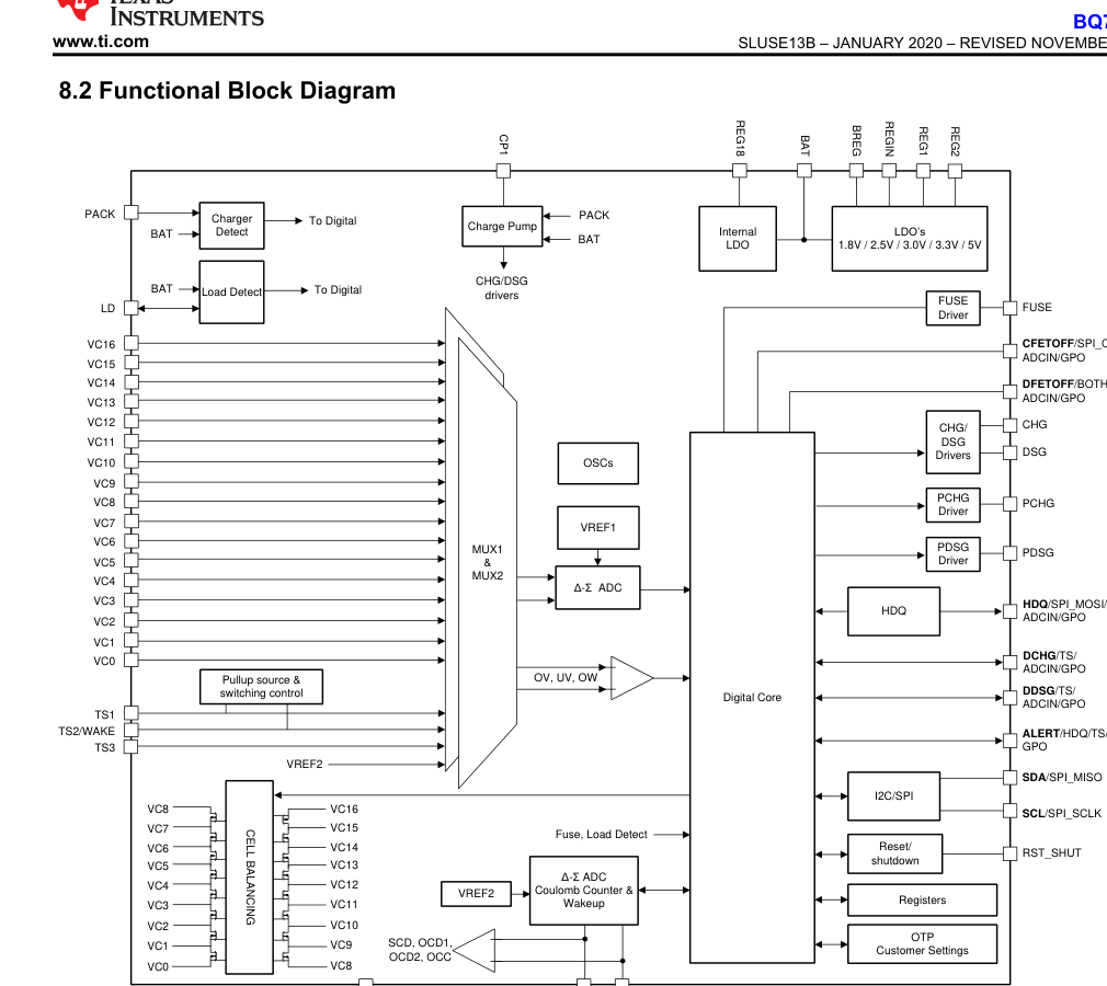
The BQ76952 is a highly integrated battery monitor and protection IC for 3-series to 16-series Li-ion, Li-polymer, and LiFePO4 battery packs. It combines high-accuracy cell and pack measurements, coulomb counting, configurable protection logic, autonomous or host-controlled cell balancing, and high-side FET gate-drive support in a 48-pin TQFP package.
Alongside measurement and protection functions, the device integrates a charge pump for CHG and DSG NFET control, precharge and predischarge drivers, a secondary fuse driver, dual programmable LDOs for external circuitry, and host communications over I2C, SPI, or HDQ. The BQ76952 family also includes factory-configured variants that change the default communications mode and REG1 startup behavior.
Device Comparison Table
| Part Number | Default Interface | CRC Enabled | REG1 Default |
|---|---|---|---|
| BQ76952 | I2C | No | Disabled |
| BQ7695201 | SPI | Yes | Disabled |
| BQ7695202 | I2C | Yes | Enabled, 3.3 V |
| BQ7695203 | SPI | Yes | Enabled, 5 V |
| BQ7695204 | SPI | Yes | Enabled, 3.3 V |
Key Specifications
Features
- • Battery monitoring capability for 3-series to 16-series cells
- • Extensive protection coverage for voltage, temperature, current, fuse, and internal diagnostics
- • Two independent ADC paths for synchronized voltage and current sampling
- • Autonomous or host-controlled cell balancing
- • Integrated charge pump for high-side NFET protection control
- • Integrated precharge, predischarge, and secondary chemical fuse drive support
- • High-voltage tolerance up to 85 V on battery-stack related pins
- • Random cell attach sequence tolerance for production environments
- • Customer-programmable OTP memory for manufacturing-time configuration
- • Dual programmable LDOs for external host and support circuitry
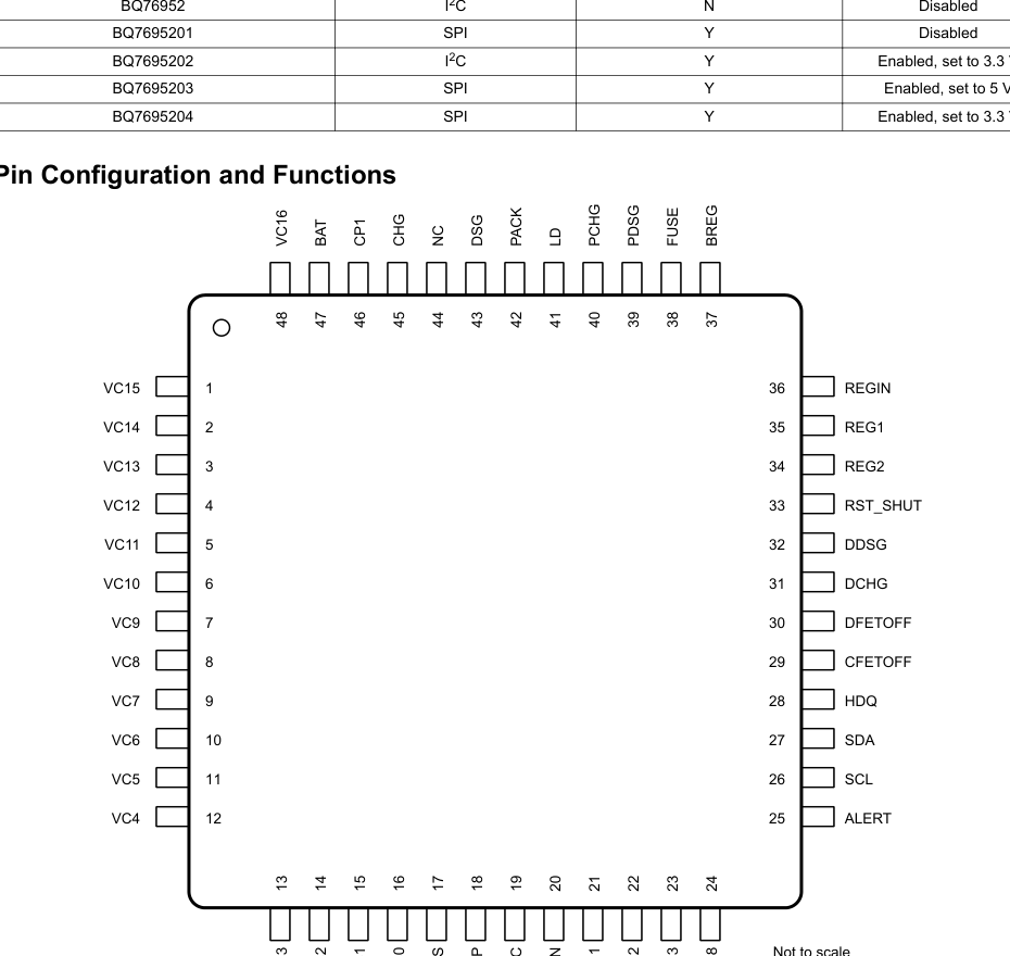
Pin Configuration
Source: Texas Instruments BQ76952 Datasheet (SLUSE13B) Manufacturer: Texas Instruments Document: SLUSE13B — Revised November 2021 Part Number: BQ76952 Package: PFB (48-pin TQFP), 7 mm × 7 mm
Absolute Maximum Ratings
| Parameter | Min | Max | Unit |
|---|---|---|---|
| BAT supply voltage | VSS - 0.3 | VSS + 85 | V |
| PACK, LD input voltage | VSS - 0.3 | VSS + 85 | V |
| PCHG, PDSG input voltage | max(VBAT - 10, VLD - 10) | VSS + 85 | V |
| FUSE input voltage | VSS - 0.3 | min(VSS + 20, VBAT + 0.3) | V |
| REG1, REG2, RST_SHUT, ALERT, SCL, SDA, HDQ, CFETOFF, DFETOFF, DCHG, DDSG | VSS - 0.3 | VSS + 6 | V |
| SRP, SRN | VSS - 0.3 | VREG18 + 0.3 | V |
Recommended Operating Conditions
| Parameter | Min | Typ | Max | Unit |
|---|---|---|---|---|
| BAT supply voltage | 4.7 | — | 80 | V |
| OTP programming supply voltage | 10 | — | 12 | V |
| PACK, LD input range | 0 | — | 80 | V |
| Current-sense differential range (SRP - SRN) | -0.2 | — | 0.2 | V |
| External cell input resistance | 20 | — | 100 | Ω |
| External cell input capacitance | 0.1 | 0.22 | 1 | µF |
| Operating temperature | -40 | — | 85 | °C |
Electrical Characteristics
| Parameter | Conditions | Min | Typ | Max | Unit |
|---|---|---|---|---|---|
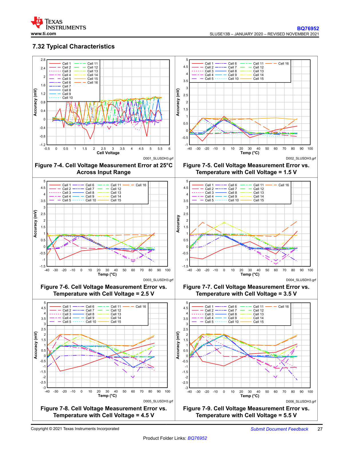
| Cell voltage measurement accuracy | 2 V < VCELL < 5 V, TA = 25°C | -5 | — | 5 | mV |
| Cell voltage measurement accuracy | 2 V < VCELL < 5 V, TA = 0°C to 60°C | -10 | — | 10 | mV |
| Cell voltage measurement accuracy | -0.2 V < VCELL < 5.5 V, TA = -40°C to 85°C | -15 | — | 15 | mV |
| Stack voltage measurement accuracy | 0 V < VC16 - VSS < 80 V | -0.5 | — | 0.5 | V |
| PACK pin voltage measurement accuracy | 0 V < VPACK < 80 V | -0.5 | — | 0.5 | V |
| LD pin voltage measurement accuracy | 0 V < VLD < 80 V | -0.5 | — | 0.5 | V |
| Coulomb counter input range | VSRP - VSRN | -0.2 | — | 0.2 | V |
| Coulomb counter effective input resistance | — | — | 2 | — | MΩ |
| Current-wake threshold error | Threshold setting between ±0.5 mV and ±5 mV | -200 | — | 200 | µV |
| ADC input range, cell differential mode | Internal VREF1 | -0.2 | — | 5.5 | V |
Power Consumption
| Mode | Conditions | Typ | Max | Unit |
|---|---|---|---|---|
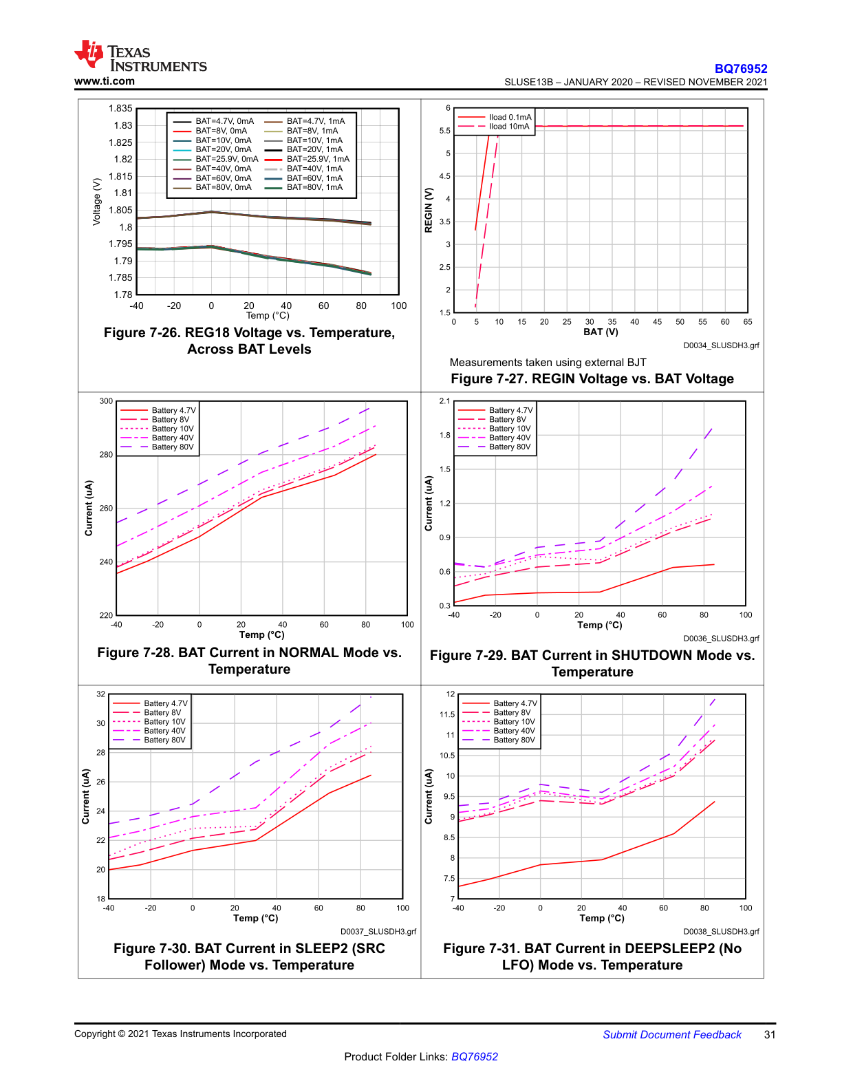
| Normal | Regular measurements and protections active | 286 | — | µA |
| Sleep 1 | Periodic protections and monitoring, DSG on in 11 V overdrive mode | 41 | — | µA |
| Sleep 2 | Periodic protections and monitoring, DSG in source-follower mode | 24 | — | µA |
| Deep sleep 1 | No monitoring or protections, LFO on | 10.7 | — | µA |
| Deep sleep 2 | No monitoring or protections, LFO off | 9.2 | — | µA |
| Shutdown | TS2 wake circuit active, no monitoring or communications | 1 | 3.1 | µA |
Power Domains
| Rail / Block | Configuration | Range / Nominal | Notes |
|---|---|---|---|
| REG18 | Internal LDO | 1.6 V to 2.0 V, 1.8 V typ | Reference rail for low-voltage functions and thermistor/ADC domains |
| REG1 | Programmable LDO | 1.8 V, 2.5 V, 3.0 V, 3.3 V, or 5.0 V nominal; up to 45 mA load | Can power an external MCU or support circuitry |
| REG2 | Programmable LDO | 1.8 V, 2.5 V, 3.0 V, 3.3 V, or 5.0 V nominal; up to 45 mA load | Independent second LDO for auxiliary rails |
| REG0 / BREG / REGIN path | Preregulator | Internal BREG-controlled preregulator or external 5.5 V REGIN supply | Feeds REG1 and REG2 |
| Charge pump / CP1 | Gate-drive boost | Supports CHG and DSG high-side NFET drive | Startup and load behavior depend on CP1 capacitance |
Thermal Information
| Package | RθJA | RθJC(top) | RθJB | ΨJT | ΨJB | Unit |
|---|---|---|---|---|---|---|
| PFB (48-pin TQFP) | 66.0 | 19.6 | 29.3 | 0.8 | 29.1 | °C/W |
Communication Interface
| Interface | Notes | Pin Mapping |
|---|---|---|
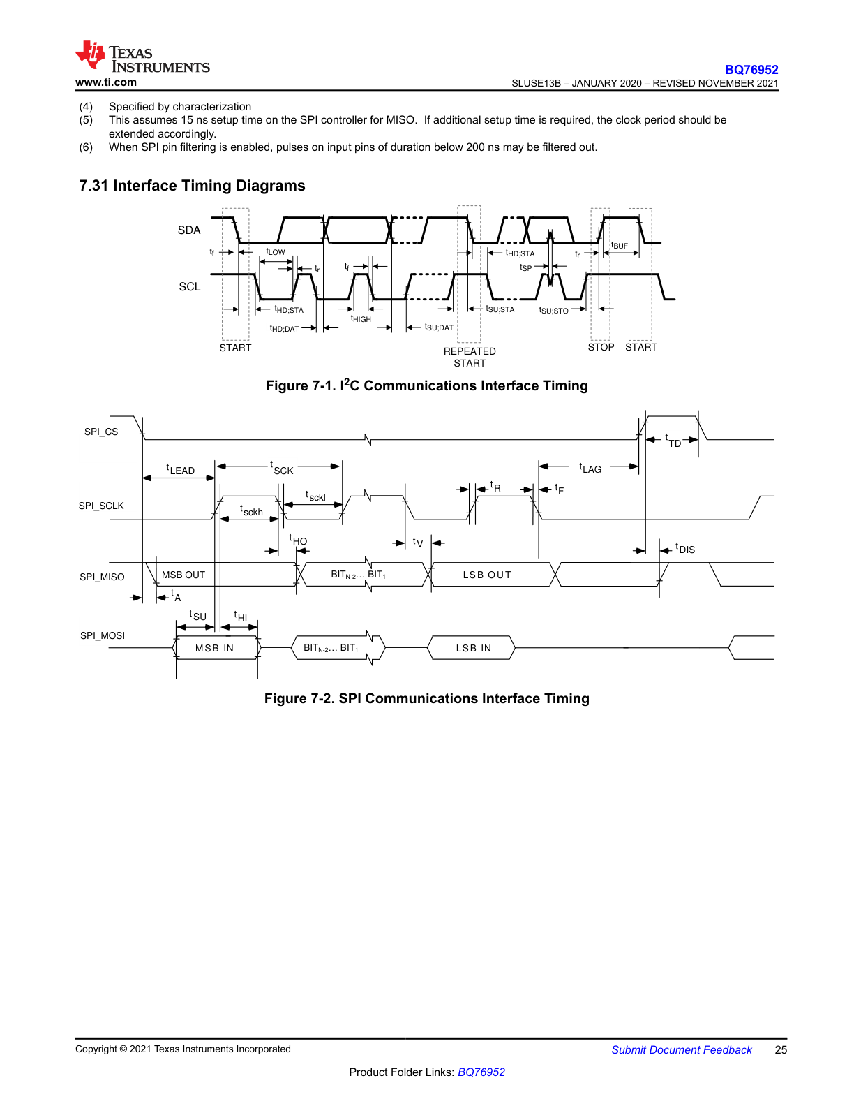
| I2C | Supports 100 kHz and 400 kHz operation; base BQ76952 defaults to I2C without CRC | `SDA`, `SCL` |
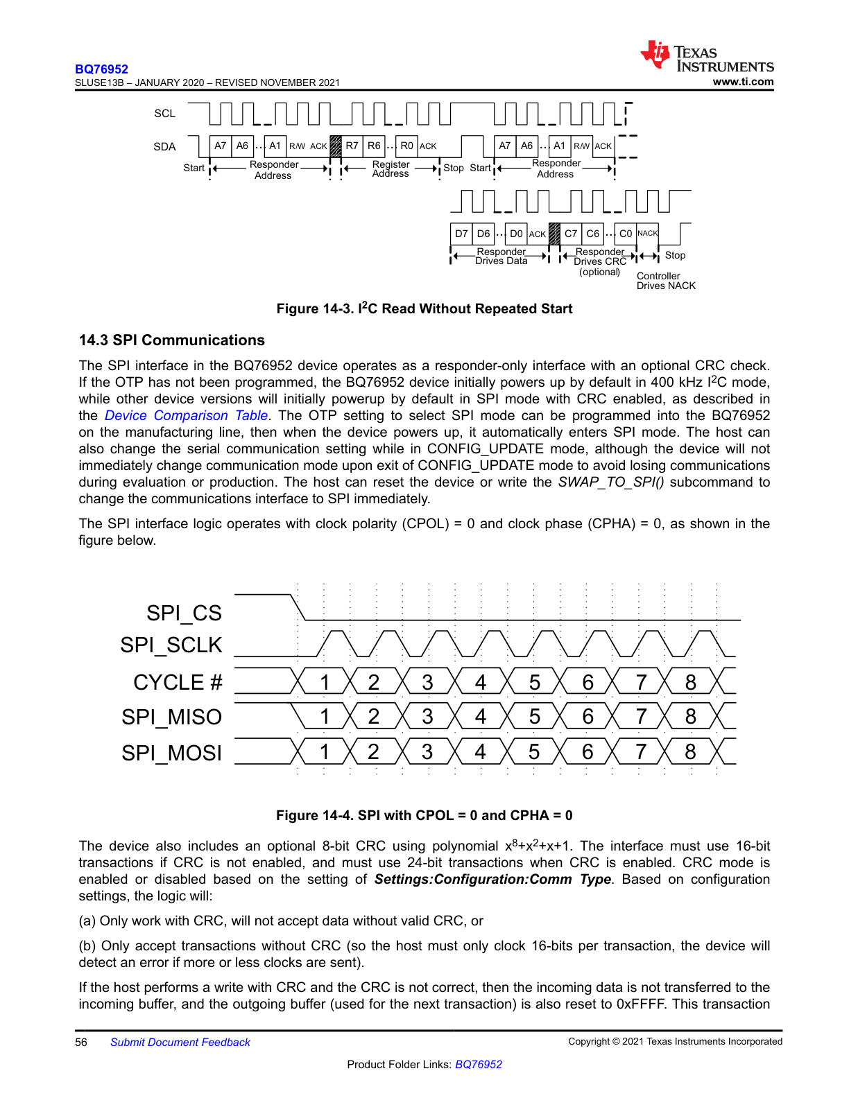
| SPI | Responder-only interface with optional CRC; uses CPOL = 0 and CPHA = 0 | `SDA` = MISO, `SCL` = SCLK, `HDQ` = MOSI, `CFETOFF` = CS |
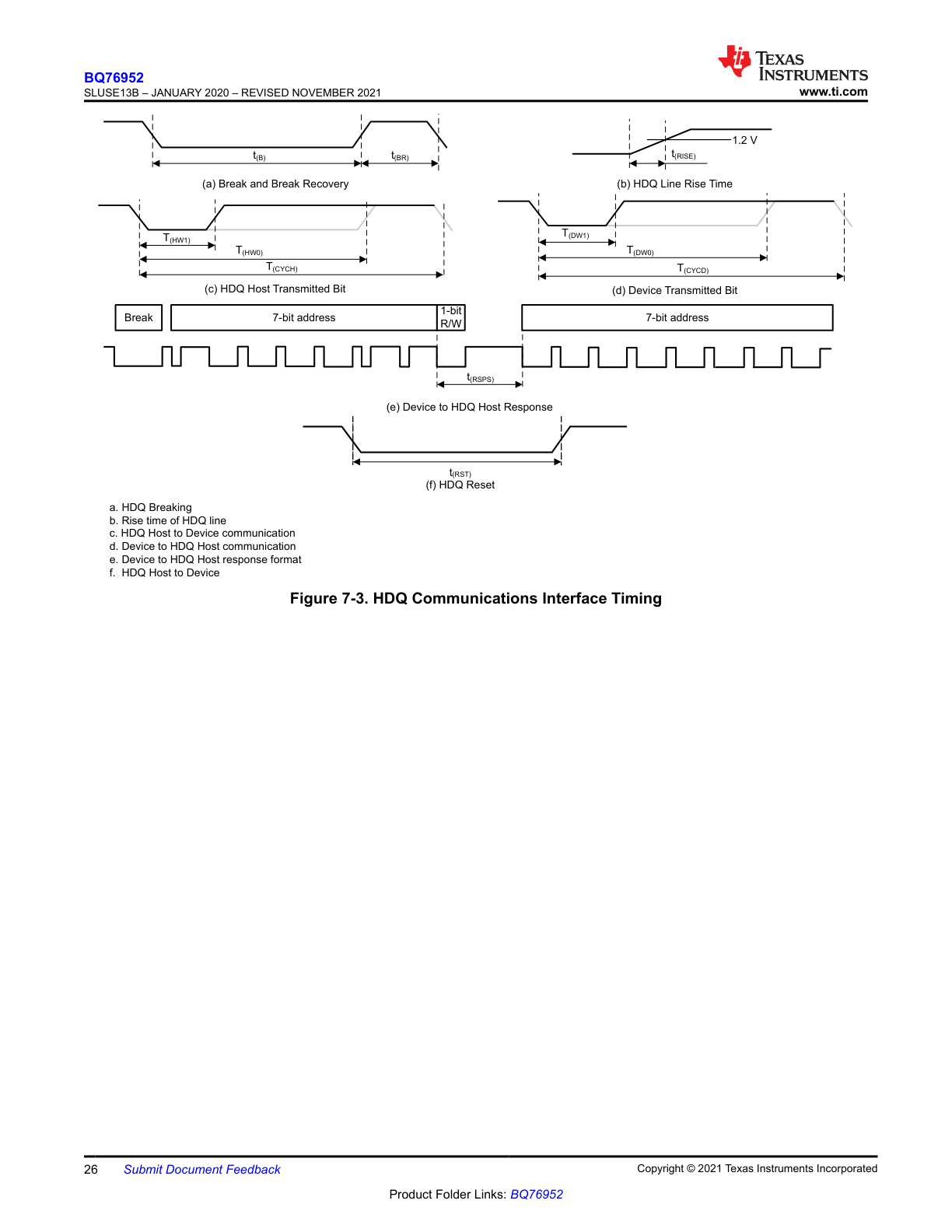
| HDQ | Single-wire asynchronous responder interface with open-drain signaling | `HDQ` or `ALERT`, depending on configuration |
Serial Transaction Coverage
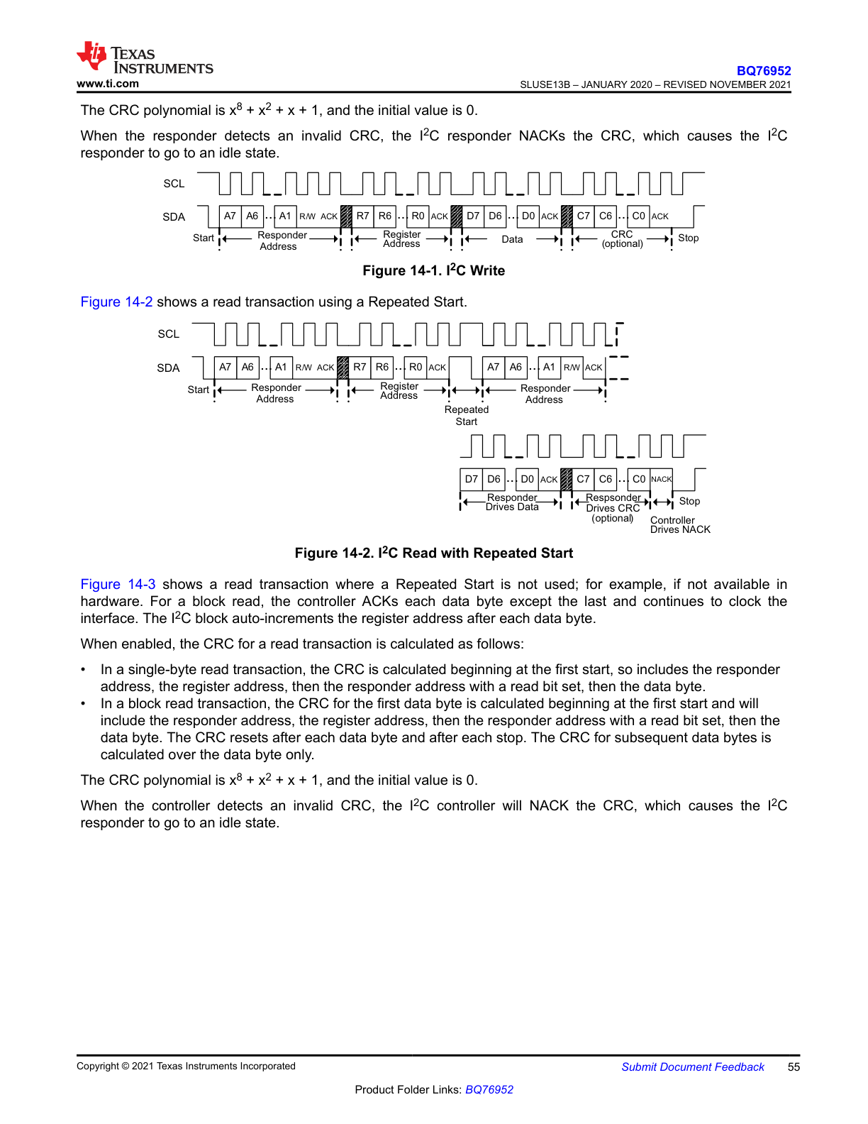
- I2C timing requirements are provided for 100 kHz and 400 kHz operation, including repeated-start and non-repeated-start read sequences.
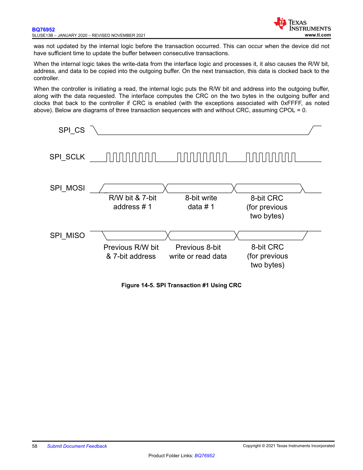
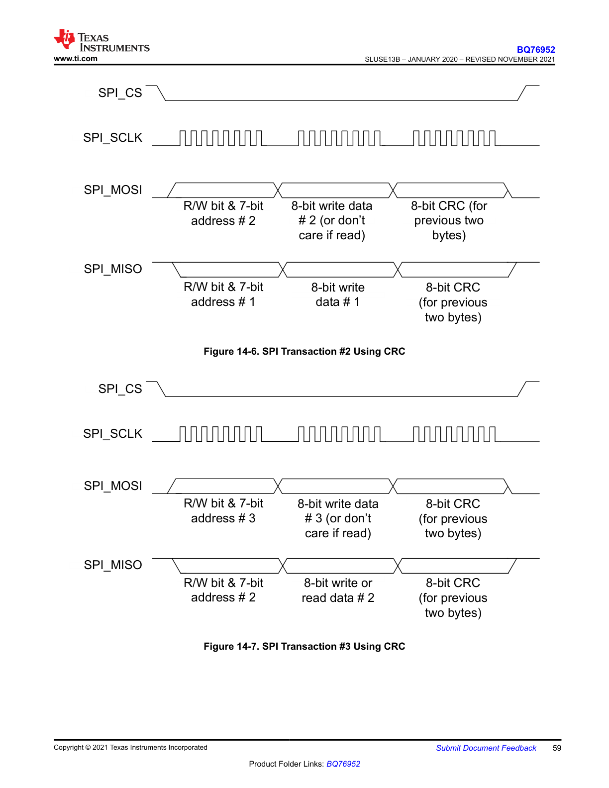
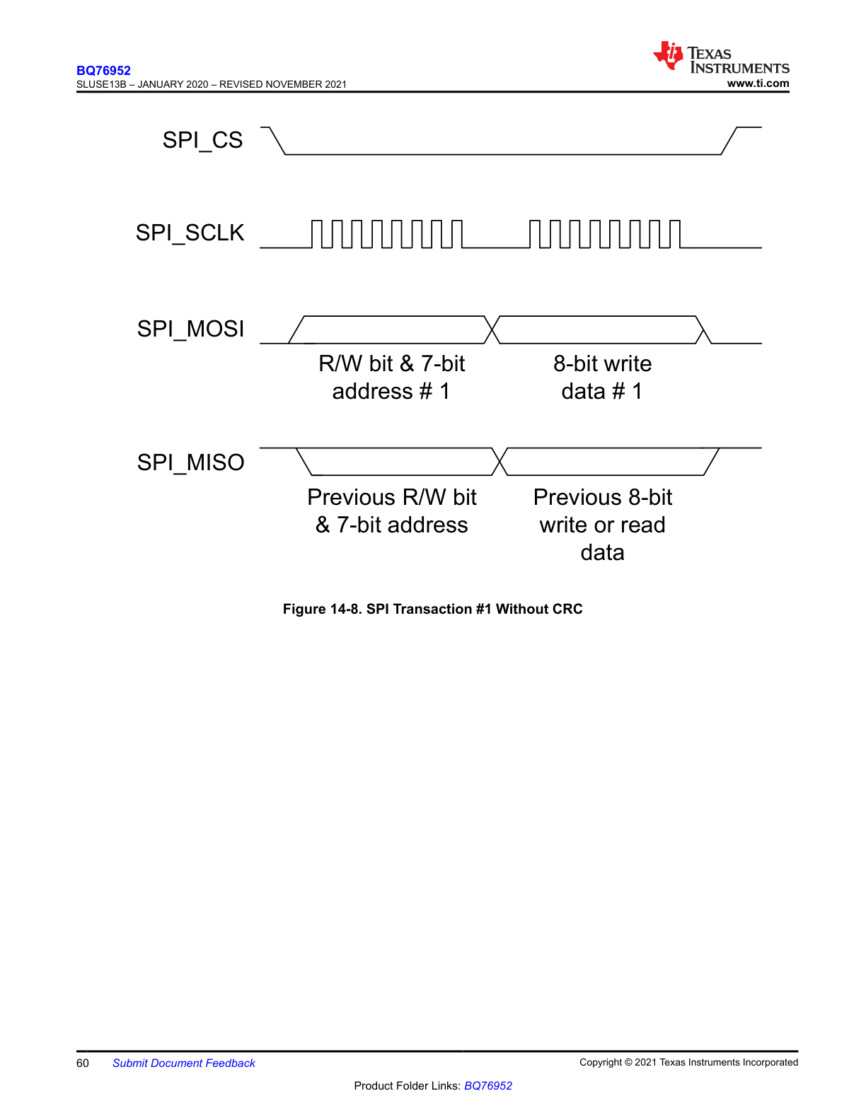
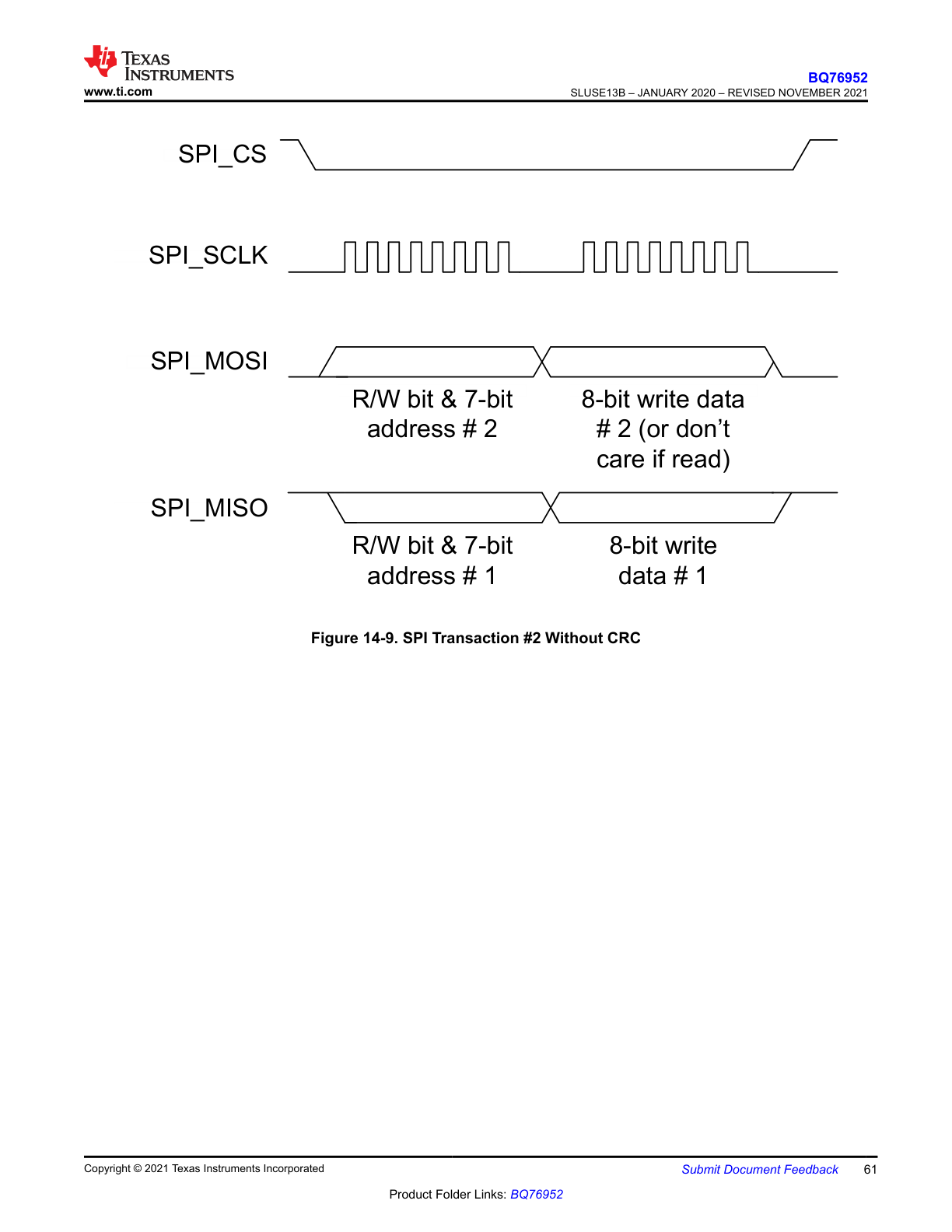
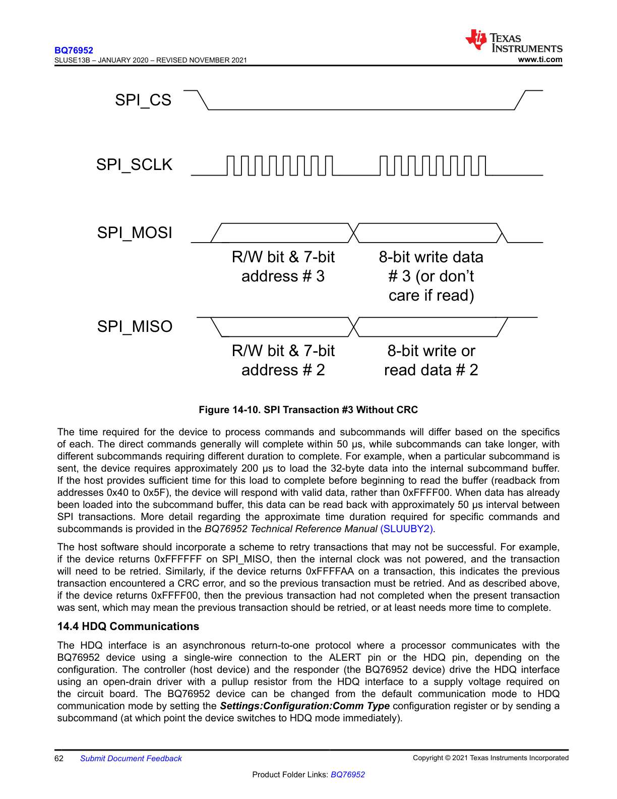
- SPI timing is documented with and without CRC, including responder timing, bus-reset behavior, and MISO drive considerations.
- HDQ is documented as a responder-only single-wire protocol with explicit break, command, and response timing.
Measurement Subsystem
| Function | Summary |
|---|---|
| Cell voltage ADC | Measures up to 16 differential cell voltages in a 3s to 16s stack; recommended input range is -0.2 V to 5.5 V per cell channel |
| Measurement loop | Scans all 16 cells, then auxiliary nodes such as VC16, PACK, LD, internal references, and enabled thermistor / ADCIN inputs |
| Loop timing | Each voltage slot takes about 3 ms, or 1.5 ms with fast ADC enabled; a full loop is typically 18 to 21 slots |
| Current measurement | Dedicated coulomb-counter ADC measures shunt voltage continuously over a ±200 mV range |
| CC1 / CC2 / CC3 filters | CC1 provides lower-rate integrated-current data, CC2 provides fast current data, and CC3 averages a programmable number of CC2 samples |
| Synchronized measurements | Current samples can be paired with cell voltage measurements for impedance analysis and diagnostics |
| ADCIN inputs | TS1, TS2, TS3, ALERT, HDQ, CFETOFF, DFETOFF, DCHG, and DDSG can be repurposed as auxiliary ADC inputs when not used for digital functions |
Protection Architecture
| Protection group | Coverage |
|---|---|
| Primary protections | Cell undervoltage / overvoltage, overcurrent in charge, multiple overcurrent-in-discharge tiers, short circuit in discharge, charge/discharge temperature protections, internal and FET overtemperature, watchdog, and precharge timeout |
| Secondary protections | Permanent-fail checks for safety cell voltage, safety current, safety temperature, imbalance, OTP / ROM / reference / oscillator faults, commanded PF, and other critical diagnostics |
| FET control | Supports autonomous, partially autonomous, or host-managed CHG / DSG FET control |
| Fuse behavior | Permanent fail can flag only, latch off FETs, or assert the `FUSE` output to permanently disable the pack |
| Driver topology | Integrated charge pump drives high-side NFET charge and discharge FETs; also supports precharge and predischarge PFET control |
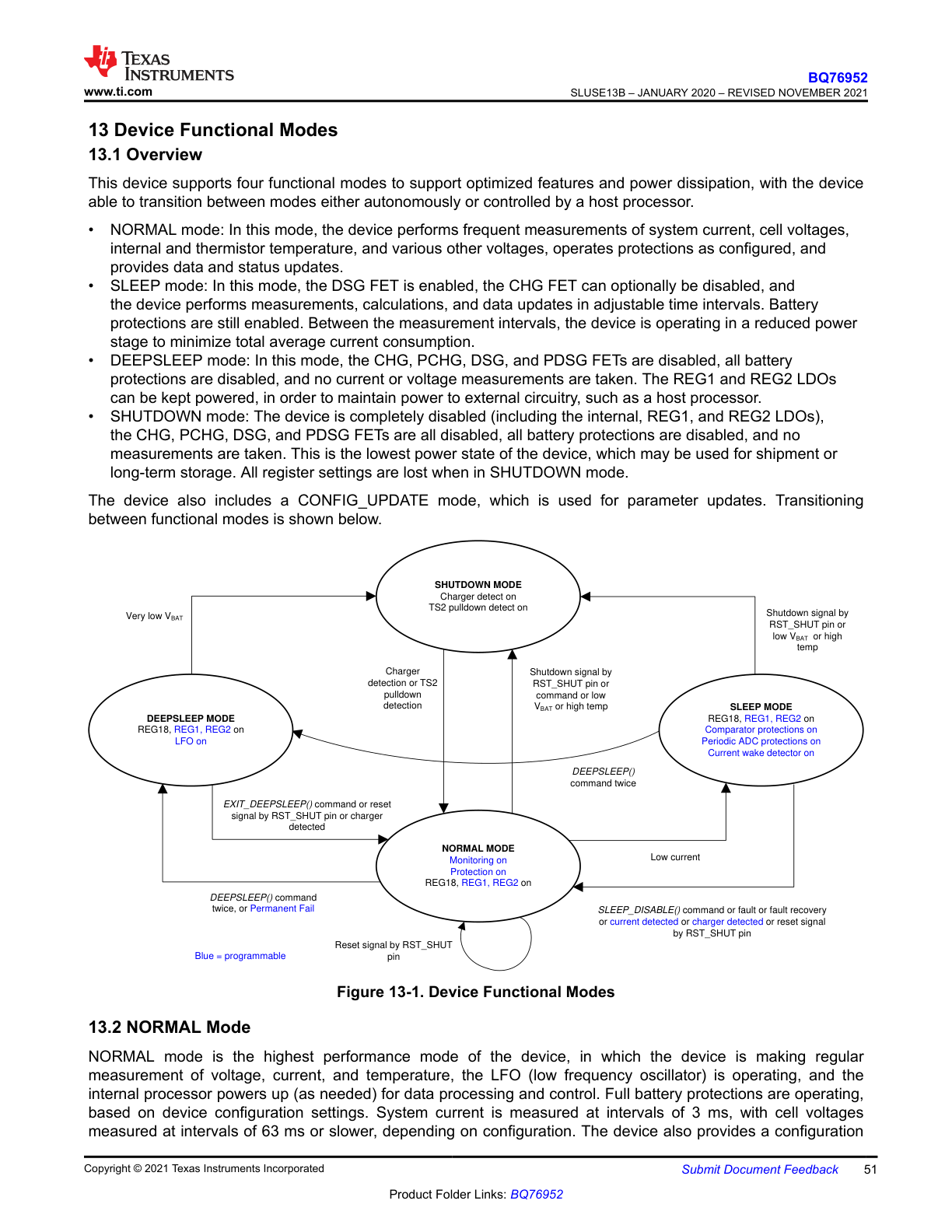
Device Functional Modes
| Mode | Behavior |
|---|---|
| NORMAL | Full measurements, protections, communications, and active pack-management behavior |
| SLEEP | Reduced-power monitoring with periodic measurements and configurable wake behavior |
| DEEPSLEEP | Lower-power standby with monitoring/protection largely disabled, preserving configuration/state as applicable |
| SHUTDOWN | Minimum-current mode with TS2 / LD based wake mechanisms and communications off |
| CONFIG_UPDATE | Register/configuration update mode used during setup and manufacturing configuration |
Cell Balancing
- Supports passive cell balancing using integrated bypass switches or external bypass FETs.
- Can operate in autonomous voltage-based balancing mode or under explicit host control.
- Autonomous balancing is limited to non-adjacent active cells; host-controlled balancing can drive adjacent cells.
- Balancing is temporarily paused around affected ADC measurements to protect voltage accuracy.
- Configuration can limit the maximum number of simultaneously balanced cells to control device heating.
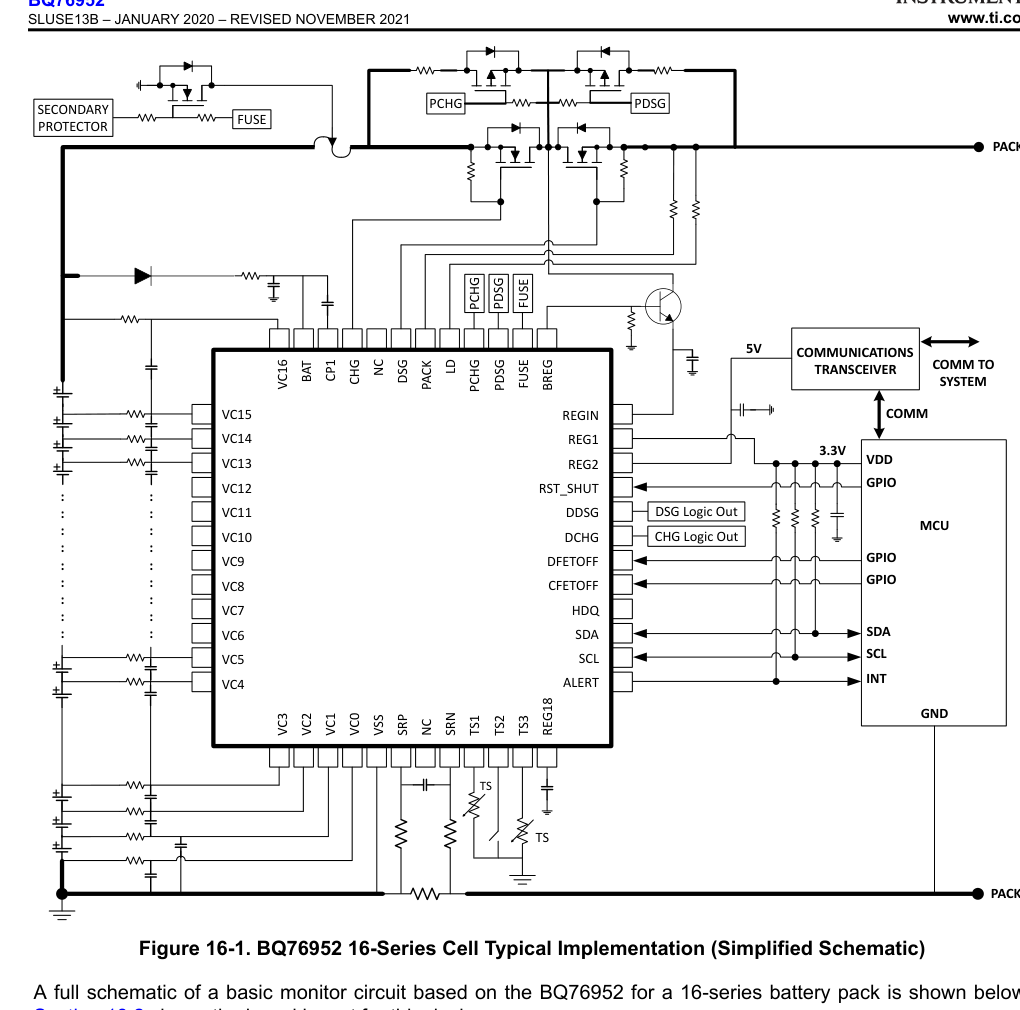
Typical Implementation
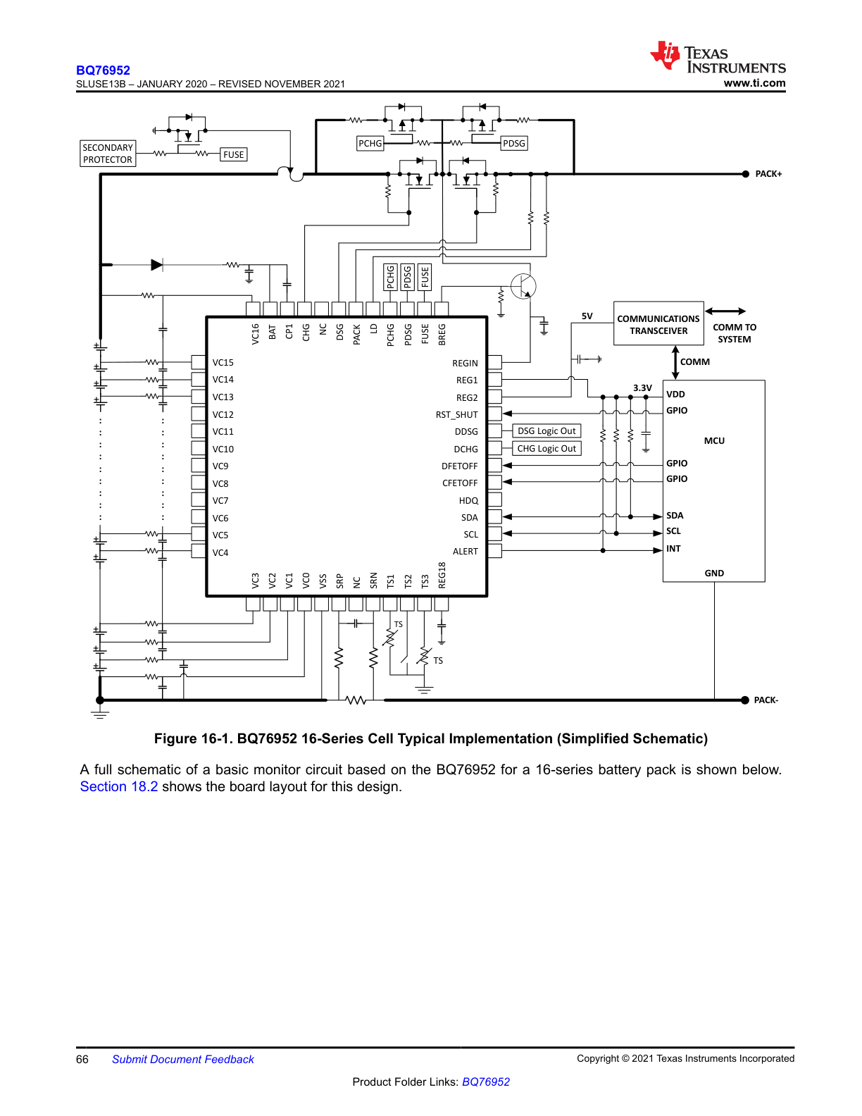
The reference application in the datasheet shows the BQ76952 in a 16-series battery pack with an external secondary protector, host MCU, and communications transceiver. The example design uses CHG and DSG high-side FETs in series, plus dedicated precharge and predischarge PFET paths, and routes the REG1 / REG2 rails to support external logic.
Key implementation notes called out by TI include:
- Keep the BAT pin alive during short-circuit events using a diode-plus-capacitor hold-up network.
- Size the CP1 capacitor based on gate charge and acceptable charge-pump startup time.
- Use symmetric SRP / SRN Kelvin routing with 100-ohm series resistors and a 0.1-uF differential filter capacitor.
- Use Battery Management Studio during development to build and validate a golden image before programming OTP.
Packages
| Package | Pins | Body Size | Notes |
|---|---|---|---|
| PFB (TQFP) | 48 | 7 mm × 7 mm | Orderable base device includes BQ76952PFBR and BQ76952PFBR.A |
Layout Guidelines
- Use true Kelvin sensing at the shunt resistor, and choose a low-drift shunt (TI calls out 50 ppm or better).
- Place the SRP / SRN filter network close to the IC, not at the shunt.
- Decouple
REG18with its required capacitor as close to the pin as possible. - Keep cell-input RC networks consistent and connect every unused VC pin either to an adjacent VC node or to a valid measurement/interconnect network.
- Consider additional ESD hardening on the I2C pins with external protection and series resistance.
Unused Pin Guidance
| Pins | Recommendation |
|---|---|
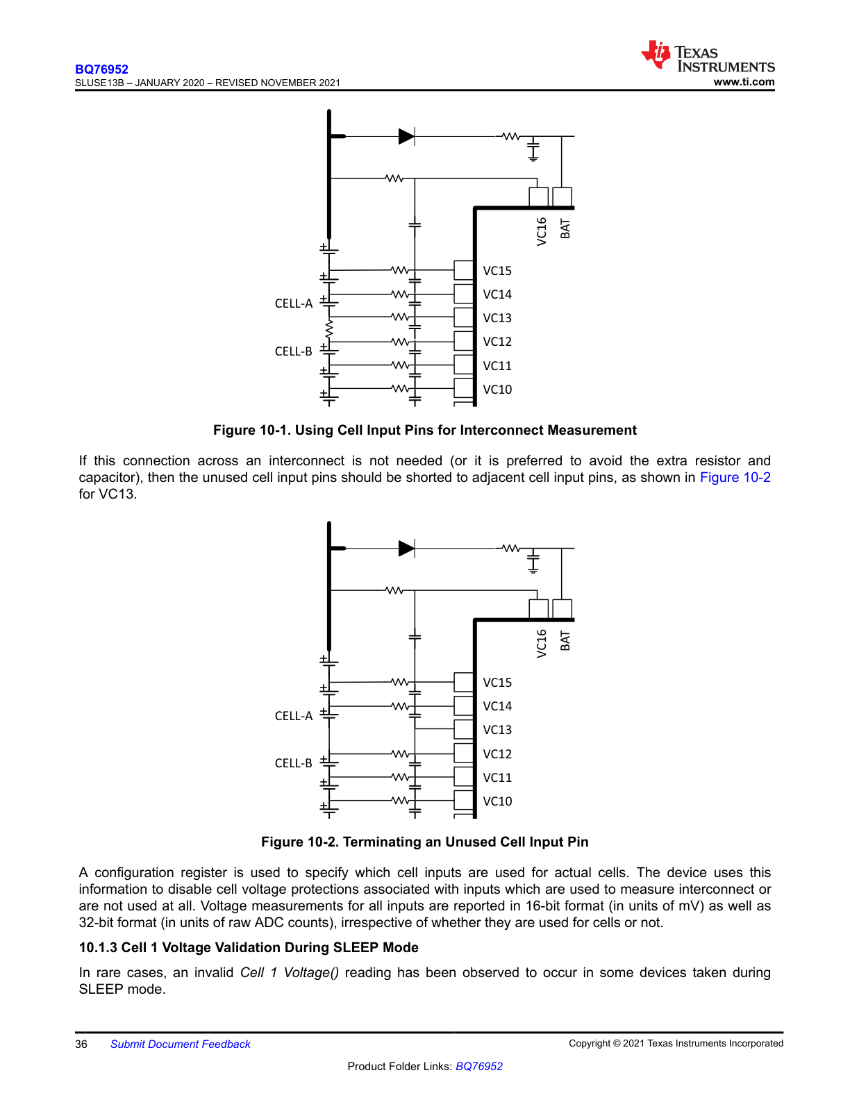
| VC0-VC16 | Every cell pin must be tied to an adjacent VC node, a real cell through RC filtering, or an interconnect measurement network |
| SRP, SRN | Tie to `VSS` if unused |
| NC pins | Leave floating or tie to a neighboring node / `VSS` |
| TS1, TS3, ALERT, HDQ, CFETOFF, DFETOFF, DCHG, DDSG | May be left floating or tied to `VSS` if unused |
| TS2 | Leave floating if shutdown wake is needed; otherwise may be left floating or tied to `VSS` |
| RST_SHUT | Tie to `VSS` if unused |
| REG1, REG2 | May be left floating or tied to `VSS` if unused |
| REGIN | Tie to `VSS` if unused |
| BREG | Tie to `VSS` if `REGIN` is also unused, otherwise tie to `REGIN` |
| FUSE | May be left floating or tied to `VSS` if unused |
| PDSG, PCHG, DSG, CHG | Leave floating if unused |
| LD | If DSG is unused, may be tied through a resistor to `PACK+` or tied to `VSS` |
| CP1 | Tie to `BAT` if unused; note the extra charge-pump current if enabled |
Diagram Coverage
The source datasheet contains 57 captioned figures across 26 figure-bearing pages. The wiki gallery for this page now includes every one of those 26 pages as screenshots, plus the hero image and supporting cropped reference images.
Extracted Figure Pages
| Datasheet Page | Coverage | Uploaded Asset |
|---|---|---|
| 25 | I2C and SPI interface timing diagrams | `bq76952-p25.png` |
| 26 | HDQ communications timing diagram | `bq76952-p26.png` |
| 27 | Cell voltage accuracy characteristic plots | `bq76952-p27.png` |
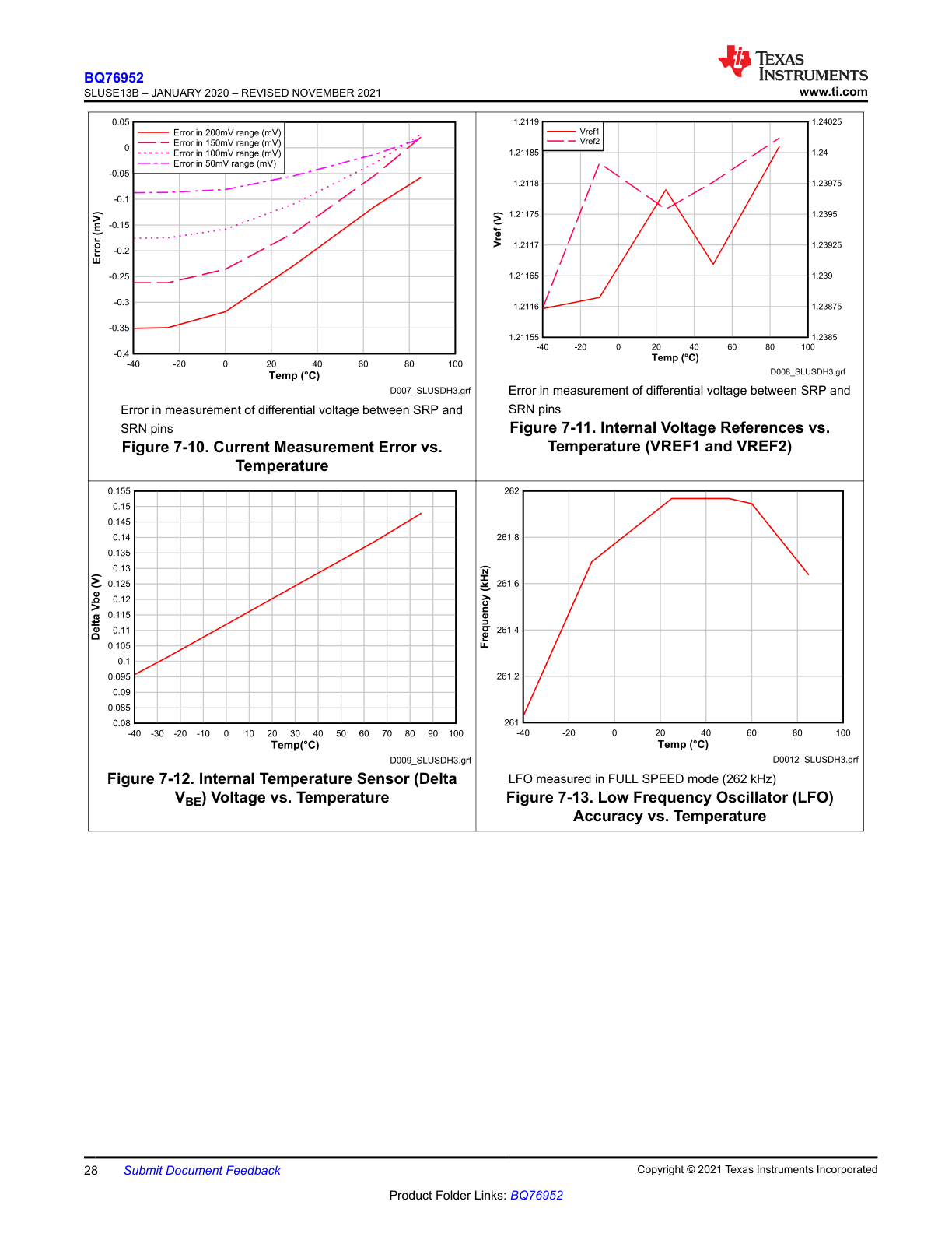
| 28 | Current, reference, temperature, and LFO characteristic plots | `bq76952-p28.png` |
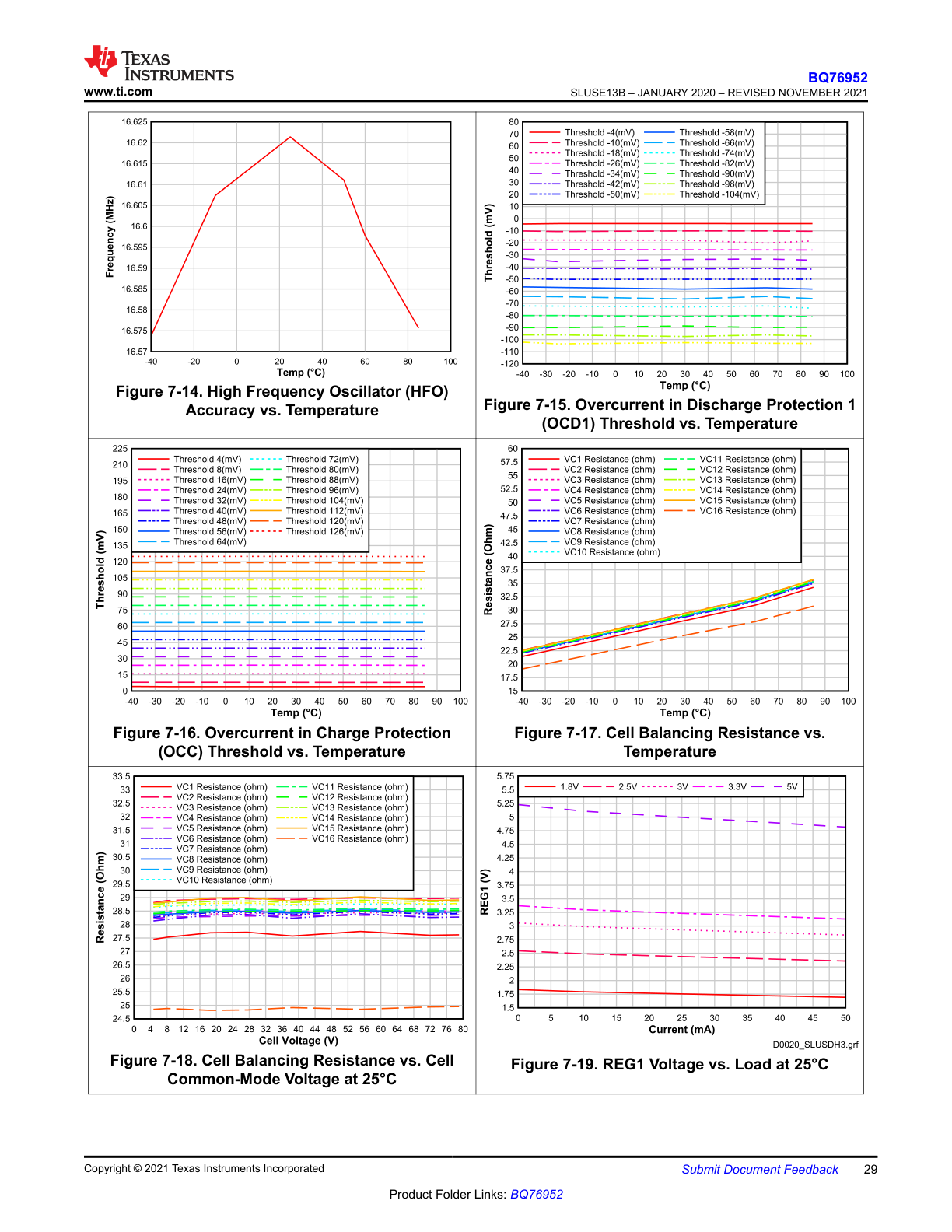
| 29 | HFO, overcurrent, balancing, and REG1 characteristic plots | `bq76952-p29.png` |
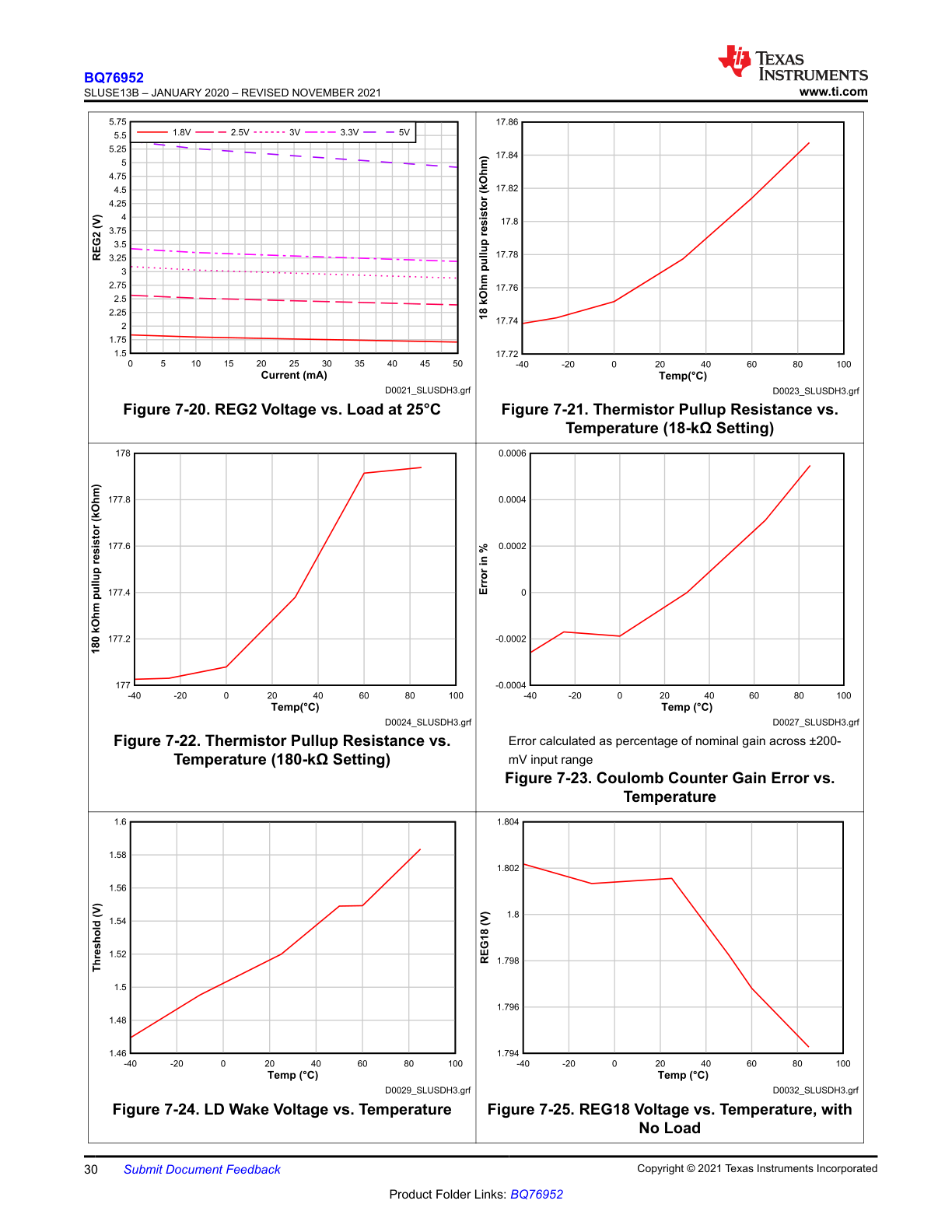
| 30 | REG2, thermistor, coulomb counter, and REG18 characteristic plots | `bq76952-p30.png` |
| 31 | REG18, REGIN, and low-power current characteristic plots | `bq76952-p31.png` |
| 36 | Cell-input interconnect and unused-pin examples | `bq76952-p36.png` |
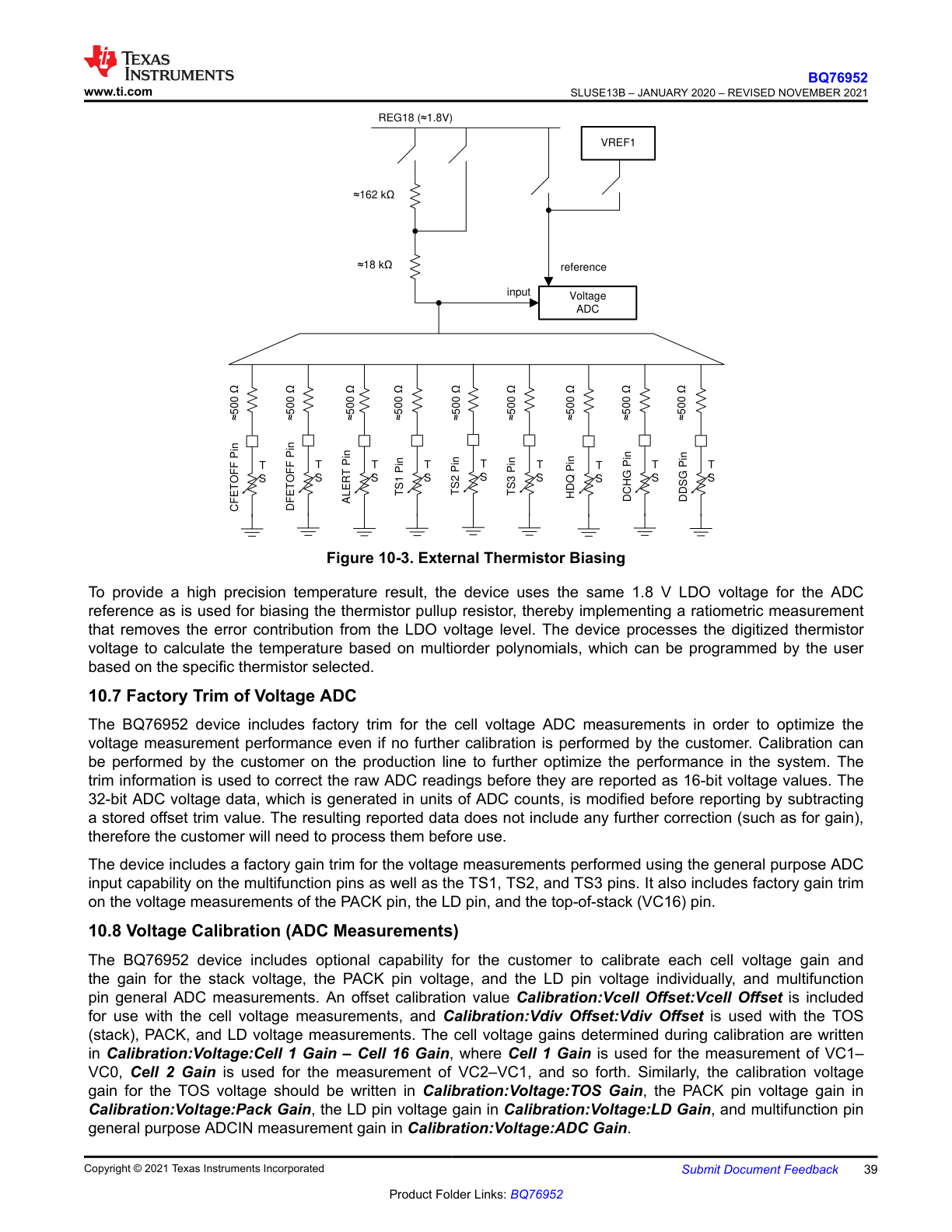
| 39 | External thermistor biasing example | `bq76952-p39.png` |
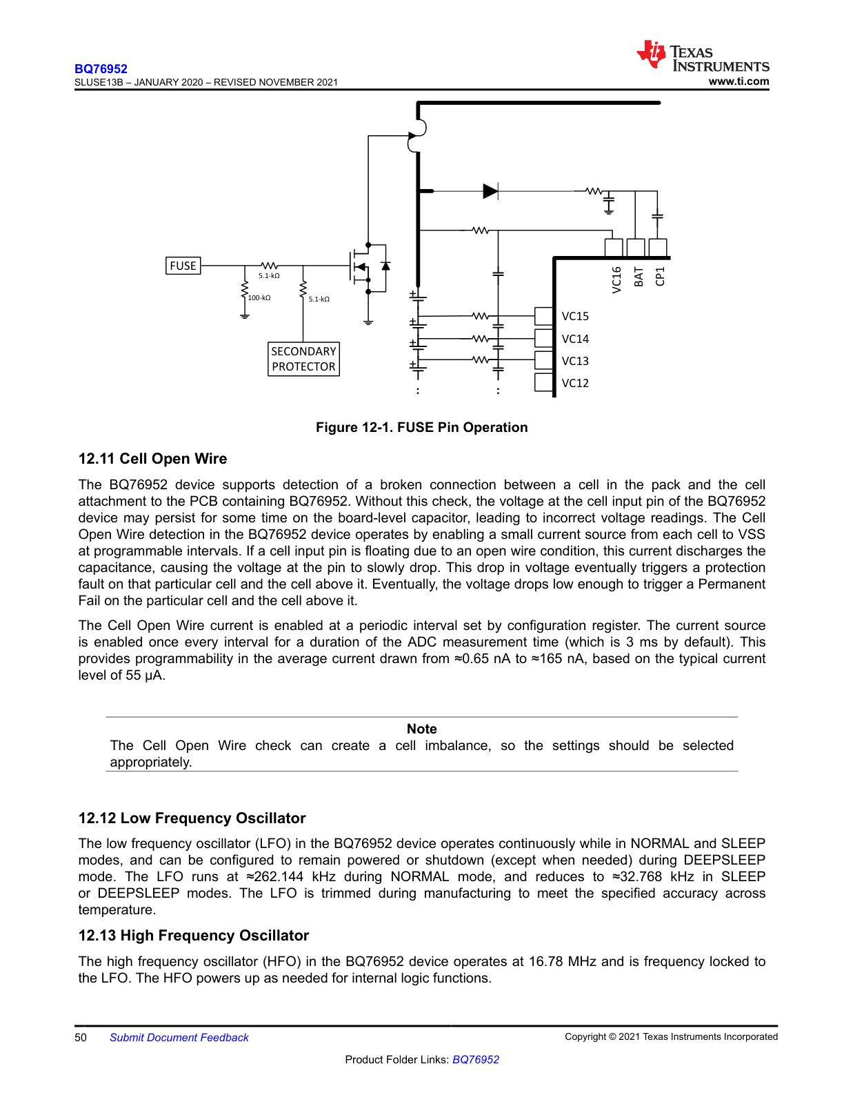
| 50 | FUSE pin operation | `bq76952-p50.png` |
| 51 | Device functional modes | `bq76952-p51.png` |
| 55 | I2C write and repeated-start read transactions | `bq76952-p55.png` |
| 56 | I2C read without repeated start and SPI mode timing | `bq76952-p56.png` |
| 58 | SPI transaction with CRC | `bq76952-p58.png` |
| 59 | Additional SPI CRC transaction timing | `bq76952-p59.png` |
| 60 | SPI transaction without CRC | `bq76952-p60.png` |
| 61 | Additional SPI non-CRC transaction timing | `bq76952-p61.png` |
| 62 | SPI transaction timing without CRC final example | `bq76952-p62.png` |
| 66 | 16-series typical implementation schematic page | `bq76952-p66.png` |
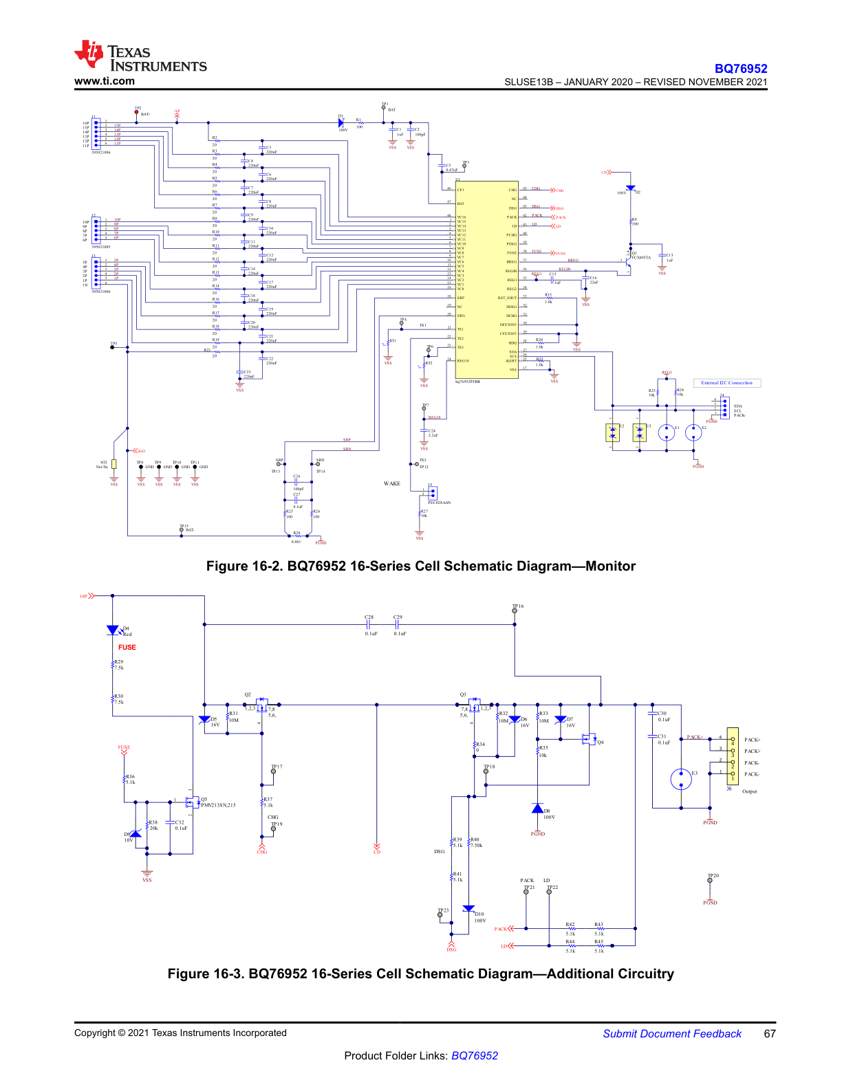
| 67 | Full 16-series monitor and additional circuitry schematics | `bq76952-p67.png` |
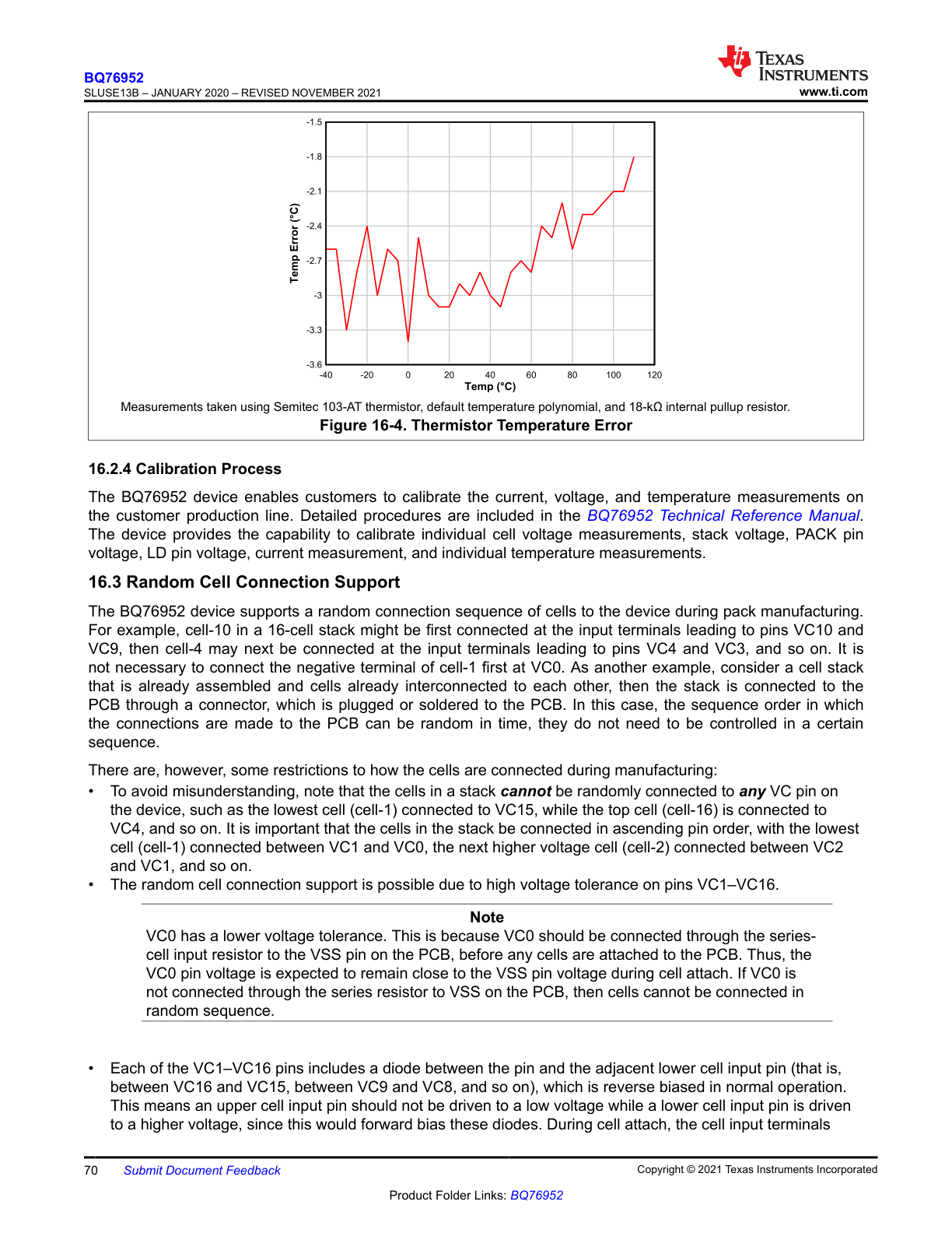
| 70 | Thermistor temperature error plot and random cell connection guidance | `bq76952-p70.png` |
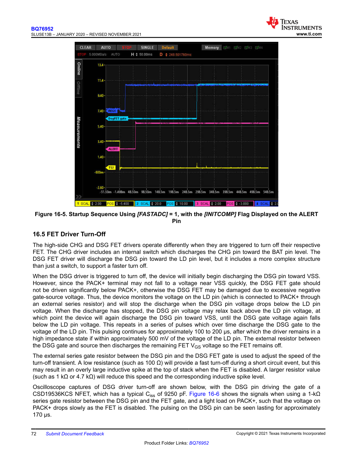
| 72 | Startup sequence timing | `bq76952-p72.png` |
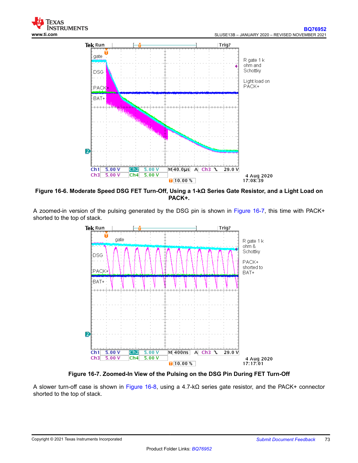
| 73 | Moderate-speed DSG FET turn-off behavior | `bq76952-p73.png` |
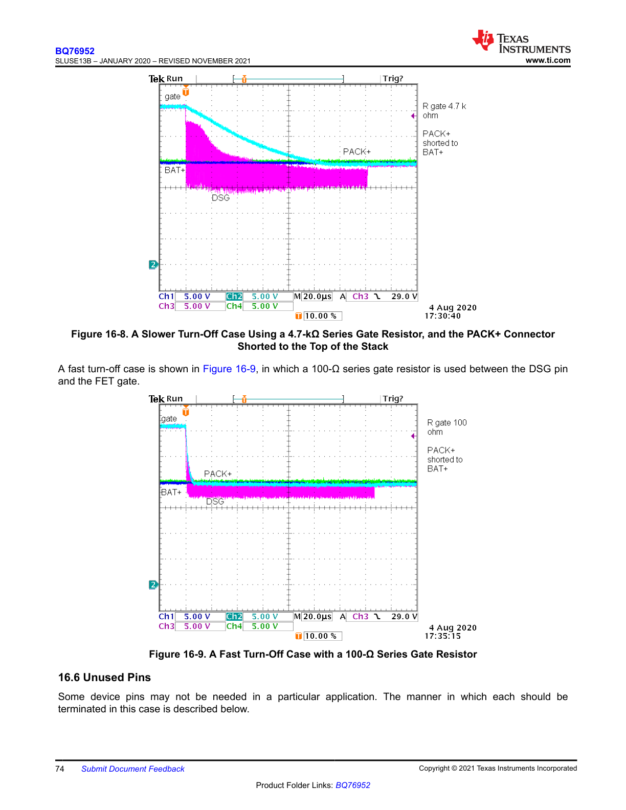
| 74 | Slow and fast DSG FET turn-off cases | `bq76952-p74.png` |
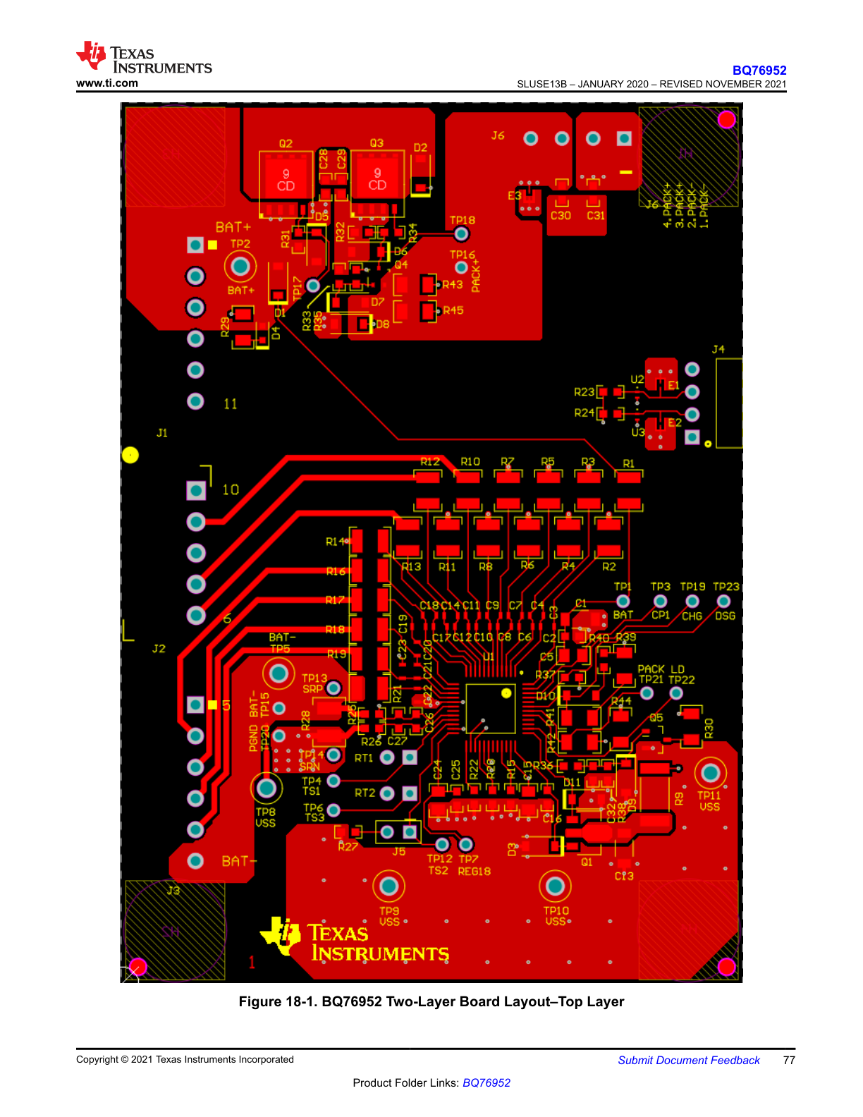
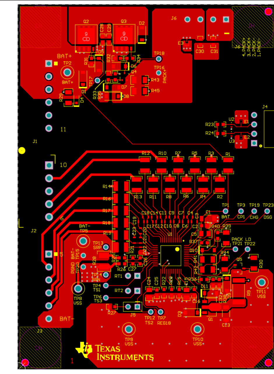
| 77 | Two-layer board layout top layer page | `bq76952-p77.png` |
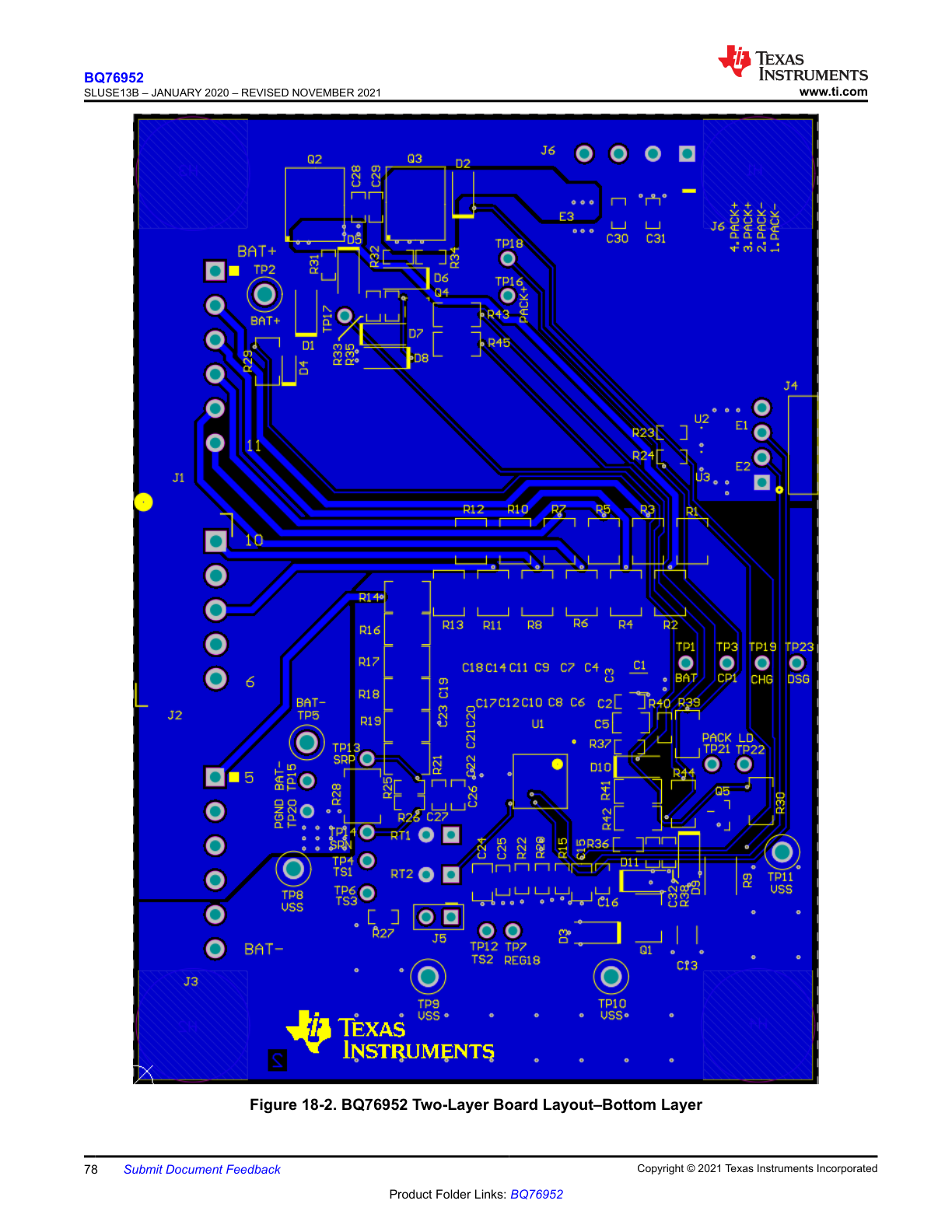
| 78 | Two-layer board layout bottom layer | `bq76952-p78.png` |
Applications
- Battery backup units
- E-bike, e-scooter, and other light electric vehicle battery packs
- Cordless power tools and garden tools
- Non-military drones
- Industrial battery packs, especially 10S and above
- Host-managed or standalone battery-management systems using high-side FET protection
Example Design Requirements
| Design Parameter | Example Value |
|---|---|
| Minimum system operating voltage | 40 V |
| Cell minimum operating voltage | 2.5 V |
| Series cell count | 16 |
| Sense resistor | 1 mΩ |
| Number of thermistors | 3 |
| Charge voltage | 68 V |
| Maximum charge current | 8 A |
| Peak discharge current | 20 A |
| OV threshold / delay | 4.30 V / 500 ms |
| UV threshold / delay | 2.5 V / 20 ms |
| SCD threshold / delay | 80 mV / 50 µs |
| OCC threshold / delay | 8 mV / 160 ms |
| OTD / OTC thresholds | 60°C / 45°C |
| UTD / UTC thresholds | -20°C / 0°C |
| REG1 usage | 3.3 V output for external host |
Detailed Design Notes
- TI's example sizing flow chooses the shunt value by balancing normal current range, short-circuit thresholds, heat dissipation, and margin; the worked example lands on a 1 mΩ, 50 ppm, 1 W shunt.
- Charge-pump overdrive is selected based on FET
VGStolerance and theRDS(on)target; 11 V drive gives lowerRDS(on), while 5.5 V can reduce gate-leakage-related current draw. - The external preregulator transistor on
BREG/REGINmust withstand the full pack charging voltage and support the expectedREG1load current. - The datasheet's example design assumes OTP programming of the final protection and operating configuration during production.
Diagrams & Graphs (30)
# BQ76952 — Parsed Datasheet

**Source:** [Texas Instruments BQ76952 Datasheet (SLUSE13B)](https://www.ti.com/lit/ds/symlink/bq76952.pdf)
**Manufacturer:** Texas Instruments
**Document:** SLUSE13B — Revised November 2021
**Part Number:** BQ76952
**Package:** PFB (48-pin TQFP), 7 mm × 7 mm

## Description

The BQ76952 is a highly integrated battery monitor and protection IC for 3-series to 16-series Li-ion, Li-polymer, and LiFePO4 battery packs. It combines high-accuracy cell and pack measurements, coulomb counting, configurable protection logic, autonomous or host-controlled cell balancing, and high-side FET gate-drive support in a 48-pin TQFP package.

Alongside measurement and protection functions, the device integrates a charge pump for CHG and DSG NFET control, precharge and predischarge drivers, a secondary fuse driver, dual programmable LDOs for external circuitry, and host communications over I2C, SPI, or HDQ. The BQ76952 family also includes factory-configured variants that change the default communications mode and REG1 startup behavior.

### Device Comparison Table

| Part Number | Default Interface | CRC Enabled | REG1 Default |
| --- | --- | --- | --- |
| BQ76952 | I2C | No | Disabled |
| BQ7695201 | SPI | Yes | Disabled |
| BQ7695202 | I2C | Yes | Enabled, 3.3 V |
| BQ7695203 | SPI | Yes | Enabled, 5 V |
| BQ7695204 | SPI | Yes | Enabled, 3.3 V |

## Key Specifications

| Parameter | Value |
| --- | --- |
| Supported battery stack | 3 to 16 series Li-ion, Li-polymer, or LiFePO4 cells |
| BAT supply voltage | 4.7 V to 80 V |
| Cell voltage accuracy | ±5 mV typ at 25°C; ±10 mV max from 0°C to 60°C; ±15 mV max from -40°C to 85°C |
| Current-sense range | ±200 mV across the shunt resistor |
| Coulomb counter offset | < 1 µV typ (feature summary) |
| Communications | I2C up to 400 kHz, SPI, HDQ one-wire |
| Programmable LDOs | REG1 and REG2 selectable to 1.8 V, 2.5 V, 3.0 V, 3.3 V, or 5.0 V |
| Low-power modes | 286 µA normal, 24 µA to 41 µA sleep, 9.2 µA to 10.7 µA deep sleep, 1 µA typ shutdown |
| Temperature sensing | Internal temperature sensor plus support for up to nine external thermistors |
| Package | PFB 48-pin TQFP, 7 mm × 7 mm |

## Features

- Battery monitoring capability for 3-series to 16-series cells
- Extensive protection coverage for voltage, temperature, current, fuse, and internal diagnostics
- Two independent ADC paths for synchronized voltage and current sampling
- Autonomous or host-controlled cell balancing
- Integrated charge pump for high-side NFET protection control
- Integrated precharge, predischarge, and secondary chemical fuse drive support
- High-voltage tolerance up to 85 V on battery-stack related pins
- Random cell attach sequence tolerance for production environments
- Customer-programmable OTP memory for manufacturing-time configuration
- Dual programmable LDOs for external host and support circuitry

## Pin Configuration

| Pin | Name | Type | Description |
| --- | --- | --- | --- |
| 1 | VC15 | Input | Sense input for cell 15; also balancing path for cell 15 and return path for cell 16 |
| 2 | VC14 | Input | Sense input for cell 14; also balancing path for cell 14 and return path for cell 15 |
| 3 | VC13 | Input | Sense input for cell 13; also balancing path for cell 13 and return path for cell 14 |
| 4 | VC12 | Input | Sense input for cell 12; also balancing path for cell 12 and return path for cell 13 |
| 5 | VC11 | Input | Sense input for cell 11; also balancing path for cell 11 and return path for cell 12 |
| 6 | VC10 | Input | Sense input for cell 10; also balancing path for cell 10 and return path for cell 11 |
| 7 | VC9 | Input | Sense input for cell 9; also balancing path for cell 9 and return path for cell 10 |
| 8 | VC8 | Input | Sense input for cell 8; also balancing path for cell 8 and return path for cell 9 |
| 9 | VC7 | Input | Sense input for cell 7; also balancing path for cell 7 and return path for cell 8 |
| 10 | VC6 | Input | Sense input for cell 6; also balancing path for cell 6 and return path for cell 7 |
| 11 | VC5 | Input | Sense input for cell 5; also balancing path for cell 5 and return path for cell 6 |
| 12 | VC4 | Input | Sense input for cell 4; also balancing path for cell 4 and return path for cell 5 |
| 13 | VC3 | Input | Sense input for cell 3; also balancing path for cell 3 and return path for cell 4 |
| 14 | VC2 | Input | Sense input for cell 2; also balancing path for cell 2 and return path for cell 3 |
| 15 | VC1 | Input | Sense input for cell 1; also balancing path for cell 1 and return path for cell 2 |
| 16 | VC0 | Input | Sense input for the negative terminal of cell 1; return path for cell-1 balancing current |
| 17 | VSS | Power | Device ground |
| 18 | SRP | Input | Top-side current-sense input for coulomb counting and current protections |
| 19 | NC | None | Not connected internally |
| 20 | SRN | Input | Bottom-side current-sense input for coulomb counting and current protections |
| 21 | TS1 | I/O | Thermistor input or general-purpose ADC input |
| 22 | TS2 | I/O | Thermistor input, shutdown wake input, or general-purpose ADC input |
| 23 | TS3 | I/O | Thermistor input or general-purpose ADC input |
| 24 | REG18 | Power | Internal 1.8 V LDO output/reference rail |
| 25 | ALERT | I/O | ALERT output, HDQ I/O, thermistor/ADC input, or digital output depending on configuration |
| 26 | SCL | I/O | I2C SCL or SPI SCLK |
| 27 | SDA | I/O | I2C SDA or SPI MISO |
| 28 | HDQ | I/O | HDQ I/O, SPI MOSI, thermistor/ADC input, or digital output |
| 29 | CFETOFF | I/O | Charge-FET-off input, SPI CS, thermistor/ADC input, or digital output |
| 30 | DFETOFF | I/O | Discharge-FET-off/BOTHOFF input, thermistor/ADC input, or digital output |
| 31 | DCHG | I/O | Digital charge-status output, thermistor/ADC input, or digital output |
| 32 | DDSG | I/O | Digital discharge-status output, thermistor/ADC input, or digital output |
| 33 | RST_SHUT | Input | Reset and shutdown control input |
| 34 | REG2 | Power | Programmable LDO output; selectable to 1.8 V, 2.5 V, 3.0 V, 3.3 V, or 5.0 V |
| 35 | REG1 | Power | Programmable LDO output; selectable to 1.8 V, 2.5 V, 3.0 V, 3.3 V, or 5.0 V |
| 36 | REGIN | Input | Input rail feeding REG1 and REG2 |
| 37 | BREG | Output | Base-drive/control output for the external preregulator transistor |
| 38 | FUSE | I/O | Fuse sense and fuse-drive pin |
| 39 | PDSG | Output | Predischarge PFET control output |
| 40 | PCHG | Output | Precharge PFET control output |
| 41 | LD | I/O | Load-detect input and wake-related multifunction pin |
| 42 | PACK | Input | Pack-voltage sense input |
| 43 | DSG | Output | Main NMOS discharge-FET drive |
| 44 | NC | None | Not connected internally |
| 45 | CHG | Output | Main NMOS charge-FET drive |
| 46 | CP1 | I/O | Charge-pump capacitor connection |
| 47 | BAT | Power | Primary device supply input |
| 48 | VC16 | Input | Sense input for cell 16, balancing path for cell 16, and top-of-stack measurement point |

## Absolute Maximum Ratings

| Parameter | Min | Max | Unit |
| --- | --- | --- | --- |
| BAT supply voltage | VSS - 0.3 | VSS + 85 | V |
| PACK, LD input voltage | VSS - 0.3 | VSS + 85 | V |
| PCHG, PDSG input voltage | max(VBAT - 10, VLD - 10) | VSS + 85 | V |
| FUSE input voltage | VSS - 0.3 | min(VSS + 20, VBAT + 0.3) | V |
| REG1, REG2, RST_SHUT, ALERT, SCL, SDA, HDQ, CFETOFF, DFETOFF, DCHG, DDSG | VSS - 0.3 | VSS + 6 | V |
| SRP, SRN | VSS - 0.3 | VREG18 + 0.3 | V |

## Recommended Operating Conditions

| Parameter | Min | Typ | Max | Unit |
| --- | --- | --- | --- | --- |
| BAT supply voltage | 4.7 | — | 80 | V |
| OTP programming supply voltage | 10 | — | 12 | V |
| PACK, LD input range | 0 | — | 80 | V |
| Current-sense differential range (SRP - SRN) | -0.2 | — | 0.2 | V |
| External cell input resistance | 20 | — | 100 | Ω |
| External cell input capacitance | 0.1 | 0.22 | 1 | µF |
| Operating temperature | -40 | — | 85 | °C |

## Electrical Characteristics

| Parameter | Conditions | Min | Typ | Max | Unit |
| --- | --- | --- | --- | --- | --- |
| Cell voltage measurement accuracy | 2 V < VCELL < 5 V, TA = 25°C | -5 | — | 5 | mV |
| Cell voltage measurement accuracy | 2 V < VCELL < 5 V, TA = 0°C to 60°C | -10 | — | 10 | mV |
| Cell voltage measurement accuracy | -0.2 V < VCELL < 5.5 V, TA = -40°C to 85°C | -15 | — | 15 | mV |
| Stack voltage measurement accuracy | 0 V < VC16 - VSS < 80 V | -0.5 | — | 0.5 | V |
| PACK pin voltage measurement accuracy | 0 V < VPACK < 80 V | -0.5 | — | 0.5 | V |
| LD pin voltage measurement accuracy | 0 V < VLD < 80 V | -0.5 | — | 0.5 | V |
| Coulomb counter input range | VSRP - VSRN | -0.2 | — | 0.2 | V |
| Coulomb counter effective input resistance | — | — | 2 | — | MΩ |
| Current-wake threshold error | Threshold setting between ±0.5 mV and ±5 mV | -200 | — | 200 | µV |
| ADC input range, cell differential mode | Internal VREF1 | -0.2 | — | 5.5 | V |

## Power Consumption

| Mode | Conditions | Typ | Max | Unit |
| --- | --- | --- | --- | --- |
| Normal | Regular measurements and protections active | 286 | — | µA |
| Sleep 1 | Periodic protections and monitoring, DSG on in 11 V overdrive mode | 41 | — | µA |
| Sleep 2 | Periodic protections and monitoring, DSG in source-follower mode | 24 | — | µA |
| Deep sleep 1 | No monitoring or protections, LFO on | 10.7 | — | µA |
| Deep sleep 2 | No monitoring or protections, LFO off | 9.2 | — | µA |
| Shutdown | TS2 wake circuit active, no monitoring or communications | 1 | 3.1 | µA |

## Power Domains

| Rail / Block | Configuration | Range / Nominal | Notes |
| --- | --- | --- | --- |
| REG18 | Internal LDO | 1.6 V to 2.0 V, 1.8 V typ | Reference rail for low-voltage functions and thermistor/ADC domains |
| REG1 | Programmable LDO | 1.8 V, 2.5 V, 3.0 V, 3.3 V, or 5.0 V nominal; up to 45 mA load | Can power an external MCU or support circuitry |
| REG2 | Programmable LDO | 1.8 V, 2.5 V, 3.0 V, 3.3 V, or 5.0 V nominal; up to 45 mA load | Independent second LDO for auxiliary rails |
| REG0 / BREG / REGIN path | Preregulator | Internal BREG-controlled preregulator or external 5.5 V REGIN supply | Feeds REG1 and REG2 |
| Charge pump / CP1 | Gate-drive boost | Supports CHG and DSG high-side NFET drive | Startup and load behavior depend on CP1 capacitance |

## Thermal Information

| Package | RθJA | RθJC(top) | RθJB | ΨJT | ΨJB | Unit |
| --- | --- | --- | --- | --- | --- | --- |
| PFB (48-pin TQFP) | 66.0 | 19.6 | 29.3 | 0.8 | 29.1 | °C/W |

## Communication Interface

| Interface | Notes | Pin Mapping |
| --- | --- | --- |
| I2C | Supports 100 kHz and 400 kHz operation; base BQ76952 defaults to I2C without CRC | `SDA`, `SCL` |
| SPI | Responder-only interface with optional CRC; uses CPOL = 0 and CPHA = 0 | `SDA` = MISO, `SCL` = SCLK, `HDQ` = MOSI, `CFETOFF` = CS |
| HDQ | Single-wire asynchronous responder interface with open-drain signaling | `HDQ` or `ALERT`, depending on configuration |

### Serial Transaction Coverage

- I2C timing requirements are provided for 100 kHz and 400 kHz operation, including repeated-start and non-repeated-start read sequences.
- SPI timing is documented with and without CRC, including responder timing, bus-reset behavior, and MISO drive considerations.
- HDQ is documented as a responder-only single-wire protocol with explicit break, command, and response timing.

## Measurement Subsystem

| Function | Summary |
| --- | --- |
| Cell voltage ADC | Measures up to 16 differential cell voltages in a 3s to 16s stack; recommended input range is -0.2 V to 5.5 V per cell channel |
| Measurement loop | Scans all 16 cells, then auxiliary nodes such as VC16, PACK, LD, internal references, and enabled thermistor / ADCIN inputs |
| Loop timing | Each voltage slot takes about 3 ms, or 1.5 ms with fast ADC enabled; a full loop is typically 18 to 21 slots |
| Current measurement | Dedicated coulomb-counter ADC measures shunt voltage continuously over a ±200 mV range |
| CC1 / CC2 / CC3 filters | CC1 provides lower-rate integrated-current data, CC2 provides fast current data, and CC3 averages a programmable number of CC2 samples |
| Synchronized measurements | Current samples can be paired with cell voltage measurements for impedance analysis and diagnostics |
| ADCIN inputs | TS1, TS2, TS3, ALERT, HDQ, CFETOFF, DFETOFF, DCHG, and DDSG can be repurposed as auxiliary ADC inputs when not used for digital functions |

## Protection Architecture

| Protection group | Coverage |
| --- | --- |
| Primary protections | Cell undervoltage / overvoltage, overcurrent in charge, multiple overcurrent-in-discharge tiers, short circuit in discharge, charge/discharge temperature protections, internal and FET overtemperature, watchdog, and precharge timeout |
| Secondary protections | Permanent-fail checks for safety cell voltage, safety current, safety temperature, imbalance, OTP / ROM / reference / oscillator faults, commanded PF, and other critical diagnostics |
| FET control | Supports autonomous, partially autonomous, or host-managed CHG / DSG FET control |
| Fuse behavior | Permanent fail can flag only, latch off FETs, or assert the `FUSE` output to permanently disable the pack |
| Driver topology | Integrated charge pump drives high-side NFET charge and discharge FETs; also supports precharge and predischarge PFET control |

## Device Functional Modes

| Mode | Behavior |
| --- | --- |
| NORMAL | Full measurements, protections, communications, and active pack-management behavior |
| SLEEP | Reduced-power monitoring with periodic measurements and configurable wake behavior |
| DEEPSLEEP | Lower-power standby with monitoring/protection largely disabled, preserving configuration/state as applicable |
| SHUTDOWN | Minimum-current mode with TS2 / LD based wake mechanisms and communications off |
| CONFIG_UPDATE | Register/configuration update mode used during setup and manufacturing configuration |

## Cell Balancing

- Supports passive cell balancing using integrated bypass switches or external bypass FETs.
- Can operate in autonomous voltage-based balancing mode or under explicit host control.
- Autonomous balancing is limited to non-adjacent active cells; host-controlled balancing can drive adjacent cells.
- Balancing is temporarily paused around affected ADC measurements to protect voltage accuracy.
- Configuration can limit the maximum number of simultaneously balanced cells to control device heating.

## Typical Implementation

The reference application in the datasheet shows the BQ76952 in a 16-series battery pack with an external secondary protector, host MCU, and communications transceiver. The example design uses CHG and DSG high-side FETs in series, plus dedicated precharge and predischarge PFET paths, and routes the REG1 / REG2 rails to support external logic.

Key implementation notes called out by TI include:

- Keep the BAT pin alive during short-circuit events using a diode-plus-capacitor hold-up network.
- Size the CP1 capacitor based on gate charge and acceptable charge-pump startup time.
- Use symmetric SRP / SRN Kelvin routing with 100-ohm series resistors and a 0.1-uF differential filter capacitor.
- Use Battery Management Studio during development to build and validate a golden image before programming OTP.

## Packages

| Package | Pins | Body Size | Notes |
| --- | --- | --- | --- |
| PFB (TQFP) | 48 | 7 mm × 7 mm | Orderable base device includes BQ76952PFBR and BQ76952PFBR.A |

## Applications

- Battery backup units
- E-bike, e-scooter, and other light electric vehicle battery packs
- Cordless power tools and garden tools
- Non-military drones
- Industrial battery packs, especially 10S and above
- Host-managed or standalone battery-management systems using high-side FET protection

### Example Design Requirements

| Design Parameter | Example Value |
| --- | --- |
| Minimum system operating voltage | 40 V |
| Cell minimum operating voltage | 2.5 V |
| Series cell count | 16 |
| Sense resistor | 1 mΩ |
| Number of thermistors | 3 |
| Charge voltage | 68 V |
| Maximum charge current | 8 A |
| Peak discharge current | 20 A |
| OV threshold / delay | 4.30 V / 500 ms |
| UV threshold / delay | 2.5 V / 20 ms |
| SCD threshold / delay | 80 mV / 50 µs |
| OCC threshold / delay | 8 mV / 160 ms |
| OTD / OTC thresholds | 60°C / 45°C |
| UTD / UTC thresholds | -20°C / 0°C |
| REG1 usage | 3.3 V output for external host |

### Detailed Design Notes

- TI's example sizing flow chooses the shunt value by balancing normal current range, short-circuit thresholds, heat dissipation, and margin; the worked example lands on a 1 mΩ, 50 ppm, 1 W shunt.
- Charge-pump overdrive is selected based on FET `VGS` tolerance and the `RDS(on)` target; 11 V drive gives lower `RDS(on)`, while 5.5 V can reduce gate-leakage-related current draw.
- The external preregulator transistor on `BREG/REGIN` must withstand the full pack charging voltage and support the expected `REG1` load current.
- The datasheet's example design assumes OTP programming of the final protection and operating configuration during production.

## Layout Guidelines

- Use true Kelvin sensing at the shunt resistor, and choose a low-drift shunt (TI calls out 50 ppm or better).
- Place the SRP / SRN filter network close to the IC, not at the shunt.
- Decouple `REG18` with its required capacitor as close to the pin as possible.
- Keep cell-input RC networks consistent and connect every unused VC pin either to an adjacent VC node or to a valid measurement/interconnect network.
- Consider additional ESD hardening on the I2C pins with external protection and series resistance.

### Unused Pin Guidance

| Pins | Recommendation |
| --- | --- |
| VC0-VC16 | Every cell pin must be tied to an adjacent VC node, a real cell through RC filtering, or an interconnect measurement network |
| SRP, SRN | Tie to `VSS` if unused |
| NC pins | Leave floating or tie to a neighboring node / `VSS` |
| TS1, TS3, ALERT, HDQ, CFETOFF, DFETOFF, DCHG, DDSG | May be left floating or tied to `VSS` if unused |
| TS2 | Leave floating if shutdown wake is needed; otherwise may be left floating or tied to `VSS` |
| RST_SHUT | Tie to `VSS` if unused |
| REG1, REG2 | May be left floating or tied to `VSS` if unused |
| REGIN | Tie to `VSS` if unused |
| BREG | Tie to `VSS` if `REGIN` is also unused, otherwise tie to `REGIN` |
| FUSE | May be left floating or tied to `VSS` if unused |
| PDSG, PCHG, DSG, CHG | Leave floating if unused |
| LD | If DSG is unused, may be tied through a resistor to `PACK+` or tied to `VSS` |
| CP1 | Tie to `BAT` if unused; note the extra charge-pump current if enabled |

## Diagram Coverage

The source datasheet contains 57 captioned figures across 26 figure-bearing pages. The wiki gallery for this page now includes every one of those 26 pages as screenshots, plus the hero image and supporting cropped reference images.

### Extracted Figure Pages

| Datasheet Page | Coverage | Uploaded Asset |
| --- | --- | --- |
| 25 | I2C and SPI interface timing diagrams | `bq76952-p25.png` |
| 26 | HDQ communications timing diagram | `bq76952-p26.png` |
| 27 | Cell voltage accuracy characteristic plots | `bq76952-p27.png` |
| 28 | Current, reference, temperature, and LFO characteristic plots | `bq76952-p28.png` |
| 29 | HFO, overcurrent, balancing, and REG1 characteristic plots | `bq76952-p29.png` |
| 30 | REG2, thermistor, coulomb counter, and REG18 characteristic plots | `bq76952-p30.png` |
| 31 | REG18, REGIN, and low-power current characteristic plots | `bq76952-p31.png` |
| 36 | Cell-input interconnect and unused-pin examples | `bq76952-p36.png` |
| 39 | External thermistor biasing example | `bq76952-p39.png` |
| 50 | FUSE pin operation | `bq76952-p50.png` |
| 51 | Device functional modes | `bq76952-p51.png` |
| 55 | I2C write and repeated-start read transactions | `bq76952-p55.png` |
| 56 | I2C read without repeated start and SPI mode timing | `bq76952-p56.png` |
| 58 | SPI transaction with CRC | `bq76952-p58.png` |
| 59 | Additional SPI CRC transaction timing | `bq76952-p59.png` |
| 60 | SPI transaction without CRC | `bq76952-p60.png` |
| 61 | Additional SPI non-CRC transaction timing | `bq76952-p61.png` |
| 62 | SPI transaction timing without CRC final example | `bq76952-p62.png` |
| 66 | 16-series typical implementation schematic page | `bq76952-p66.png` |
| 67 | Full 16-series monitor and additional circuitry schematics | `bq76952-p67.png` |
| 70 | Thermistor temperature error plot and random cell connection guidance | `bq76952-p70.png` |
| 72 | Startup sequence timing | `bq76952-p72.png` |
| 73 | Moderate-speed DSG FET turn-off behavior | `bq76952-p73.png` |
| 74 | Slow and fast DSG FET turn-off cases | `bq76952-p74.png` |
| 77 | Two-layer board layout top layer page | `bq76952-p77.png` |
| 78 | Two-layer board layout bottom layer | `bq76952-p78.png` |
Sub-Skills
What are Sub-Skills?
Sub-skills are community-contributed AI skill extensions for this component.
They teach AI assistants about specific tools, configurators, or workflows.
Examples:
- A manufacturer’s configuration tool for a motor controller
- A community-written design guide for an amplifier circuit
- An automated test/validation script for a sensor module
How to add one: Click Add Sub-Skill, provide the URL
to your skill and a brief description. Submissions are reviewed by the Adom team
before going live.
Sub-skills are community-contributed AI skill extensions for this component. They teach AI assistants about specific tools, configurators, or workflows.
Examples:
- A manufacturer’s configuration tool for a motor controller
- A community-written design guide for an amplifier circuit
- An automated test/validation script for a sensor module
How to add one: Click Add Sub-Skill, provide the URL to your skill and a brief description. Submissions are reviewed by the Adom team before going live.
No sub-skills yet. Be the first to contribute one!
How Claude finds this page (discovery snippet)
This page opts into Adom Wiki auto-discovery. When a user working in Claude Code mentions any of the trigger phrases below, Claude can proactively suggest this page. The pitch is exactly what Claude will say.
"bq76952 datasheet", "texas instruments battery monitor", "16s battery monitor", "battery monitor protector ic", "show me the bq76952 datasheet", "extract specs from bq76952"