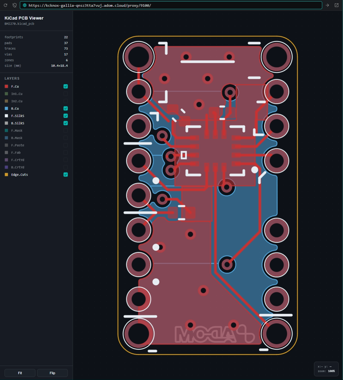
A 2D PCB viewer for .kicad_pcb files, rendered as SVG inside a Hydrogen
webview panel. For when you want to see a board without launching
KiCad on the user's desktop.

Why this exists
Adom already has 3D viewers (.glb chip models) and gerber viewers
(post-fab artwork). What was missing was the in-between: the editable
KiCad board, viewed flat, with toggleable layers, in the cloud editor.
This app is deliberately 2D — for 3D inspection, use the existing 3D viewers. Use this when:
- The user pasted a
.kicad_pcband you want to confirm it looks sane before doing anything else with it. - You're debugging a board layout and want to see "did the autorouter stack everything on F.Cu? Where are the vias?"
- You want to take a layer-isolated screenshot (e.g. board outline only) to drop into a doc, a PR, or a chat message.
- You want to verify silkscreen orientation, or check what's actually on the back side of a board, without firing up pcbnew.
Install
gh release download v0.1.0 --repo adom-inc/kicad-pcb-viewer \
    --pattern kicad-pcb-viewer-linux \
    -D /tmp
sudo install -m 0755 /tmp/kicad-pcb-viewer-linux /usr/local/bin/kicad-pcb-viewer
kicad-pcb-viewer install   # deploys SKILL.md to ~/.claude/skills/kicad-pcb-viewer/
Runs on any Python 3.10+ system. No external dependencies — just stdlib.
Quick start (human-driven)
kicad-pcb-viewer view path/to/board.kicad_pcb
Opens a Hydrogen webview tab in a non-VSCode pane (per app-creator
skill — never inside the editor pane).
| Action | Input |
|---|---|
| Pan | Click + drag |
| Zoom | Scroll wheel (toward cursor) |
| Reset to fit | Fit button |
| Mirror horizontally | Flip button |
| Toggle layer | Click a row in the sidebar |
Coordinate readout (mm) and zoom % live in the bottom-right HUD.
CLI subcommands
| Command | What it does |
|---|---|
view <path> [--port N] | Start server + open webview tab. Default. |
serve <path> [--port N] | Start server only (no tab). Useful for headless scripting. |
shutdown [--port N] | Stop a running viewer (graceful). |
install | Deploy SKILL.md to ~/.claude/skills/kicad-pcb-viewer/. |
version | Print version. |
Default port: 9100. The first positional arg is auto-inferred as view
if it ends in .kicad_pcb or is an existing path, so
kicad-pcb-viewer board.kicad_pcb works as shorthand.
Multi-layer boards
Inner copper layers (In1.Cu, In2.Cu, In3.Cu, In4.Cu) get distinct
colors and z-order. The layer panel only lists layers that actually
have geometry on this board — empty layers stay hidden, so the panel
doesn't fill up with 30 unused entries.

HTTP API — every action is AI-drivable
Per app-creator §7, the same endpoints the UI uses are reachable via
HTTP. This is the property that turns a webview into an AI surface.
| Method | Path | Description |
|---|---|---|
| GET | /state | Phase, file path, filename, stats, bbox, layer visibility. |
| GET | /board | Full parsed board JSON (footprints, pads, segments, arcs, vias, zones, gr). |
| GET | /layers | {name: {idx, kind, alias, visible}} for every layer on the board. |
| POST | /layers | Body {name: bool, ...} — set visibility for one or more layers. |
| POST | /load | Body {path: "..."} — open a different .kicad_pcb without restarting the server. |
| POST | /fit | Reset view to fit the board. |
| POST | /flip | Toggle horizontal mirror (B-side viewing). Returns {flipped: bool}. |
| GET | /console | Last 500 forwarded UI-side console messages. |
| POST | /console | Append a message (called from the UI). |
| DELETE | /console | Clear log. |
| POST | /eval | Body {code: "..."} — queue a JS snippet, returns {id}. UI runs it on next poll. |
| GET | /eval/pending | UI poller endpoint — returns {id, code} or empty. |
| GET | /eval/<id> | Read result of a prior /eval post. |
| POST | /eval/<id>/result | UI POSTs result back here (internal). |
| POST | /shutdown | Graceful exit. |
| GET | /cmds/pending | UI poller for fit/flip commands queued by /fit and /flip. |
| GET | / | The UI HTML. |
| GET | /favicon.svg | Brand icon. |
AI recipes
Self-contained scripts an AI can copy-paste. All assume the viewer is
running on port 9100 against some board.
Recipe 1 — "is this board mostly empty?"
Quick stats check before doing anything else.
kicad-pcb-viewer serve board.kicad_pcb --port 9100 &
sleep 1
curl -s http://127.0.0.1:9100/state | jq '.stats, .bbox'
# {"footprints":13,"pads":31,"segments":61,"arcs":0,"vias":6,"zones":0,"gr":16}
# {"x":18.8,"y":18.8,"w":10.4,"h":10.4}
curl -s -X POST http://127.0.0.1:9100/shutdown >/dev/null
Recipe 2 — "isolate Edge.Cuts and screenshot"
For a board-outline export. Hide every layer except the edge.
curl -X POST http://127.0.0.1:9100/layers \
    -H 'Content-Type: application/json' \
    -d '{
      "F.Cu":false,"B.Cu":false,
      "In1.Cu":false,"In2.Cu":false,"In3.Cu":false,"In4.Cu":false,
      "F.SilkS":false,"B.SilkS":false,
      "F.Mask":false,"B.Mask":false,
      "F.Paste":false,"B.Paste":false,
      "F.Fab":false,"B.Fab":false,
      "F.CrtYd":false,"B.CrtYd":false,
      "Edge.Cuts":true
    }'
adom-cli hydrogen screenshot panel --name "PCB: <filename>"
Recipe 3 — "show only the back side"
Hide front-side layers, flip the view, screenshot.
curl -X POST http://127.0.0.1:9100/layers -H 'Content-Type: application/json' \
    -d '{"F.Cu":false,"F.SilkS":false,"F.Mask":false,"F.Paste":false,"F.Fab":false,"F.CrtYd":false,
         "B.Cu":true,"B.SilkS":true,"Edge.Cuts":true}'
curl -X POST http://127.0.0.1:9100/flip
adom-cli hydrogen screenshot panel --name "PCB: <filename>"
Recipe 4 — "list every footprint and its placement"
Useful for cross-referencing with a BOM or schematic.
curl -s http://127.0.0.1:9100/board | \
    jq '.footprints[] | {refdes, value, x, y, rot, layer}'
# {"refdes":"U1","value":"BMA400","x":24.0,"y":24.0,"rot":0,"layer":"F.Cu"}
# ...
Recipe 5 — "diff two boards by stats"
for f in v1.kicad_pcb v2.kicad_pcb; do
    curl -s -X POST http://127.0.0.1:9100/load \
        -H 'Content-Type: application/json' -d "{\"path\":\"$PWD/$f\"}" >/dev/null
    echo "=== $f ==="
    curl -s http://127.0.0.1:9100/state | jq '.stats'
done
Recipe 6 — "swap to a new board without restarting"
The same server can host any board. POST /load to swap without
opening a new tab.
curl -X POST http://127.0.0.1:9100/load \
    -H 'Content-Type: application/json' \
    -d '{"path":"/home/adom/project/foo/foo.kicad_pcb"}'
adom-cli hydrogen webview refresh --name "PCB: <old-filename>"
(The tab name keeps the original board's filename — a future version can
update the title on /load.)
Recipe 7 — "inspect the rendered DOM via /eval"
Need to know what's actually visible? Eval a snippet inside the page.
curl -X POST http://127.0.0.1:9100/eval \
    -H 'Content-Type: application/json' \
    -d '{"code":"return Array.from(document.querySelectorAll(\".layer-group\")).map(g => ({layer: g.dataset.layer, hidden: g.classList.contains(\"hidden\"), elements: g.children.length}))"}'
# {"id":"a1b2c3"}

# Read result via /console (the UI logs results)
curl -s http://127.0.0.1:9100/console | jq '.messages[-1]'
Recipe 8 — "headless render-to-screenshot pipeline"
Combine serve, layer toggles, and adom-cli hydrogen screenshot to
build per-layer images for a doc:
kicad-pcb-viewer view board.kicad_pcb --port 9100 &
sleep 2
for layer in F.Cu B.Cu F.SilkS Edge.Cuts; do
    # Hide everything except this layer + Edge.Cuts (always nice to see outline)
    body=$(jq -nc --arg L "$layer" '
        {"F.Cu":false,"B.Cu":false,"In1.Cu":false,"In2.Cu":false,
         "F.SilkS":false,"B.SilkS":false,"F.Mask":false,"B.Mask":false,
         "F.Paste":false,"B.Paste":false,"F.Fab":false,"B.Fab":false,
         "F.CrtYd":false,"B.CrtYd":false,"Edge.Cuts":true} |
        .[$L] = true')
    curl -s -X POST http://127.0.0.1:9100/layers -H 'Content-Type: application/json' -d "$body" >/dev/null
    sleep 0.5
    adom-cli hydrogen screenshot panel --name "PCB: $(basename board.kicad_pcb)"
done
What it parses
(footprint …)— placement (at), rotation, child pads + graphics(pad …)—rect,roundrect,circle,oval, with drill (round or oval slot), through-hole and SMD(segment …),(arc …)— copper traces with width(via …)— size + drill(zone …)— filled polygons (post-fill state preferred, falls back to outline iffilled_polygonnot present)(gr_line/arc/circle/rect/poly …)— top-level graphics on any layer(fp_line/arc/circle/rect/poly …)— footprint-level graphics (silk, fab, courtyard)(layers …)— layer table with index, kind, alias- Pad-side
(layers …)lists with*.Cu/*.Mask/*.Pastewildcards expanded to the matching concrete layers
What it doesn't (yet)
- Schematic (
.kicad_sch) rendering — different format, different scope. - Net highlighting / cross-probing.
- File watching — call
POST /loadto reload after edits. - Refdes / value labels overlaid on the board (too cluttered at default zoom; could be added as a togglable text overlay layer).
- Bezier curves on
gr_curve— currently approximated as polylines.
Pane placement (important)
The viewer ALWAYS opens in a pane that is NOT the VSCode pane. If a non-VSCode pane already exists, the tab joins it; otherwise the VSCode pane is split vertically and the tab lands in the new pane.
This rule lives in skills/app-creator §4 — it applies to every Adom
app, not just this one. Putting webviews as sibling tabs inside the
VSCode pane covers the editor and is wrong.
Files in this repo
bin/kicad-pcb-viewer    # Python CLI (subcommands: view, serve, install, shutdown, version)
src/parser.py           # s-expression tokenizer + per-layer extractor
src/server.py           # HTTP server, all endpoints, asset loading (source + zipapp)
src/ui.html             # SVG renderer, pan/zoom, layer panel, console fwd, eval poller
docs/icon.svg           # Brand-teal favicon (also the tab icon)
docs/SKILL.md           # AI usage doc deployed by `kicad-pcb-viewer install`
samples/                # BMA400 + BMI270 reference boards (from adom-inc/bosch-molecules)
scripts/build.sh        # Builds dist/kicad-pcb-viewer-linux zipapp (~22 KB)
Repo
adom-inc/kicad-pcb-viewer — private. Releases attach a single-file
zipapp (kicad-pcb-viewer-linux).