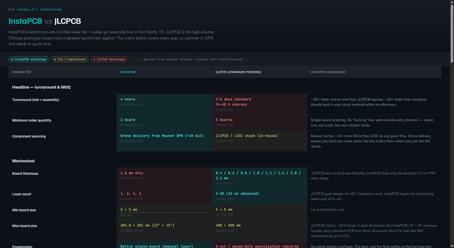
InstaPCB vs JLCPCB
Side-by-side capability comparison for Adom's in-house InstaPCB fab + assembly line vs JLCPCB, the high-volume Chinese prototype house most engineers benchmark against.
InstaPCB is Adom's UV-fiber-laser fab + stencil-free solder-jet assembly line in Fort Worth, TX. Drone-delivered components from Mouser DFW (~40 min) keep the line stocked. Boards land in your cloud workcell within 4 hours of submitting gerbers.
The interactive comparison tab below covers every spec a customer or DFM tool needs at quote time — turnaround, MOQ, mechanical envelope, conductor specs, drilled features, solder mask + silkscreen, surface finish, stackup + impedance, and assembly DFM.
Where InstaPCB wins
- Turnaround — 4 hours fab + assembly vs JLCPCB's 3-5 day standard / 24-48 h express
- MOQ — 1 board vs JLCPCB's 5-board minimum
- Min trace width — 0.08 mm (3 mil) vs JLCPCB's 0.127 mm (5 mil) on 2-layer
- Min annular ring — 0.125 mm vs JLCPCB's 0.15 mm
- Min via drill — 0.20 mm on every layer count vs JLCPCB's 0.30 mm on 2L
- Trace-to-edge clearance — 0.05 mm vs JLCPCB's 0.30 mm (laser depanel is glass-clean)
- Min silkscreen text — 0.10 mm vs JLCPCB's 1.0 mm (laser etch resolves much finer than printed silk)
- Selective V-scoring — Adom-invented: any 2D curve with designer-placed trace bridges, replaces mousebites entirely
- Edge plating — free side-effect of the laser-cut + electroplate sequence; no add-on fee
- Native single-board ordering — depanel laser cuts the final outline as the last process step
- In-line per-net electrical test — every net probed before mask + silk
Where JLCPCB wins
- Layer count — 1-20 (32 advanced) vs InstaPCB's 1, 2, 4, 6
- Board thickness flexibility — 0.4 / 0.6 / 0.8 / 1.0 / 1.2 / 1.6 / 2.0 / 3.2 mm vs InstaPCB's 1.6 mm only
- Solder mask color — 7 colors vs InstaPCB's green only
- Surface finish options — HASL / ENIG / OSP / immersion silver / tin vs InstaPCB's bare-Cu / as-plated
- Copper weight options — 0.5 / 1 / 2 / 3 oz vs InstaPCB's 0.5 oz
- Impedance control — ±10% controlled-impedance certification (microstrip / coplanar / diff-pair) vs not offered on InstaPCB today
- Max aspect ratio — 10:1 vs InstaPCB's 8:1
- Max board size — 400 × 500 mm vs InstaPCB's 304.8 × 381 mm (12" × 15")
Open the interactive comparison
Click the InstaPCB vs JLCPCB sample tab below to view the full matrix. The table has a sticky header so the column titles stay visible while scrolling, and every cell is color-coded:
- Teal — InstaPCB advantage
- Yellow — tie / parity
- Red — JLCPCB advantage
- Dashed underline — value derived from process physics (replaceable with an authoritative number once published)
Sources
JLCPCB capability values cross-referenced against jlcpcb.com/capabilities/pcb-capabilities, jlcpcb.com/pcb-fabrication/fr4-pcb, and Schemalyzer's late-2025 JLCPCB design rules guide. InstaPCB values are pulled from the canonical gallia/skills/instapcb/SKILL.md skill.
See also
- The full instapcb skill — DFM rules + design-rule defaults read by
aci-drc, chipsmith, and the InstaPCB quote form - The aci-instapcb-process skill — the 26-step manufacturing build animation
- The solder-jetting skill — Adom's stencil-free 300 µm dome dispense rules