

PCB Footprint Creator
Create professional PCB footprints, preview them interactively in the Gallia Viewer, iterate with the user, and deliver to their local KiCad or Fusion 360 Electronics via Adom Desktop Conduit.
What It Does
The footprint creator skill handles the full workflow:
- Research — Searches KiCad's 7,000+ standard footprints first, downloads matching packages, or creates from scratch using datasheet specs
- Create — Generates
.kicad_modfiles with proper pad geometry, silk screen, courtyard, fab outline, and pin 1 markers - Metadata — Builds rich pad descriptions with engineering-grade detail (voltage ranges, decoupling recommendations, etc.)
- Preview — Renders interactive FpView HTML with the KiCad CLI service for high-fidelity SVG output
- Iterate — User reviews in Gallia Viewer, requests changes, skill regenerates
- Deliver — Sends to KiCad Footprint Editor or Fusion 360 Electronics via Adom Desktop Conduit
Supported Output Formats
- KiCad (
.kicad_mod) — Native KiCad footprint file - Fusion 360 Electronics (
.lbr) — Complete EAGLE XML library with symbol + package + device connects
FpView — Interactive Footprint Viewer
FpView is the branded interactive viewer that renders footprints with:
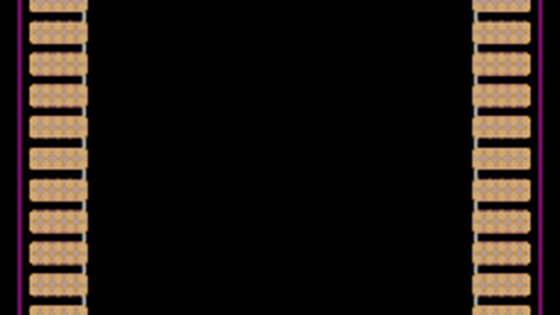
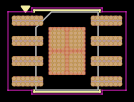
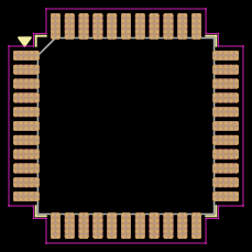
- Dark PCB-style theme with grid background
- Pad hover highlighting — teal highlight with rich tooltips showing pad number, signal name, dimensions, and description
- Click-to-pin tooltips — click a pad to lock the tooltip for text selection and link clicking
- Solder blob visualization — 250µm gold circles showing Adom's InstaPCB paste jetting pattern (toggle with S key)
- Layer toggles — Grid (G), Solder (S), Labels (L) with toolbar buttons and keyboard shortcuts
- Zoom and pan — scroll to zoom, drag to pan, F to fit, 1 to reset
- Coordinate readout — live cursor position in kicad_mod coordinate space
- Info bar — manufacturer, description, pad count, body size, courtyard, 3D model reference, datasheet link
- Regen button — shows a prompt for regenerating the viewer, auto-copies to clipboard
- Wiki edit link — "Suggest edit" button for community corrections
Solder Blob Visualization
The Solder layer shows warm gold circles representing physical solder blobs for Adom's InstaPCB paste jetting process:
- 250µm diameter blobs with 0.25mm center-to-center spacing
- Fills each SMD pad surface (thru-hole excluded)
- Respects pad rotation and boundaries
- Adjustable blob size: 250–600µm
- Placement accuracy: ±50µm
KiCad CLI Service Integration
All rendering runs on a shared remote KiCad CLI service — KiCad is NOT installed locally. The service provides:
- SVG export with accurate solder mask, copper fills, and layer rendering
- GLB/STEP 3D model export
- Design Rule Check (DRC)
- 7,000+ standard footprint library search and download
Lint and Validation
Every footprint passes through:
- Design rule linter — courtyard present, fab outline, pin 1 marker, courtyard clearance ≥0.25mm, no silk-pad overlap
- Artifact validator — all required files exist (
.kicad_mod, metadata JSON, SVG, FpView HTML, README), pad counts match, descriptions complete
Package Types Supported
Works with any package type — from tiny 0402 passives to 100+ pin QFPs:
| Category | Examples |
|---|---|
| Passives | 0402, 0603, 0805, 1206 |
| Transistors | SOT-23, SOT-223, DPAK |
| Small IC | SOIC-8, TSSOP, MSOP |
| Large IC | QFP, LQFP, TQFP (44-100+ pins) |
| BGA/LGA | LGA-14, QFN-48, BGA |
| Sensors | Custom packages (VL53L0X, BMI423) |
| Connectors | USB-C, JST, pin headers |