
altium-pcblib
πŸ’¬ Sample prompts Paste any of these into Claude Code to use this skill
Add to Cargo Add altium-pcblib to my Cargo.toml as a git dependency
Render SVG Render the parser's authoritative SVG for an Altium .PcbLib file
Compare to KiCad Compare the Altium .PcbLib pad layout to the KiCad .kicad_mod for a chip and tell me where they disagree
Debug rotation Why are my altium pads rotated 90 degrees wrong in chipsmith?
Pick variant This .PcbLib has multiple variants β€” pick the one whose pad count matches the kicad footprint
⚑ Install this skill

Paste this into Claude Code (VS Code panel, Adom editor, or terminal) to install:

Search the Adom Wiki for the skill "altium-pcblib" (slug: altium-pcblib) at https://wiki-ufypy5dpx93o.adom.cloud/wiki/skills/altium-pcblib and install it into my local ~/.claude/skills/altium-pcblib/ directory. Fetch the skill_source content from the wiki page and save it as SKILL.md. Then confirm it's installed by showing the first 5 lines.
?
What is a skill? Skills are instructions that teach AI assistants like Claude Code how to perform specific tasks. The description below is loaded into the AI as context when you invoke this skill. Well-written skills make the AI significantly more effective. Like Wikipedia, anyone can improve a skill by clicking Edit AI Skill — or have your AI submit an edit on your behalf.

Screenshots

Description

Edit AI Skill

What this is

altium-pcblib is a private Adom Rust crate that reads Altium Designer's binary footprint libraries (.PcbLib, and the PCB stream embedded inside .IntLib) and emits per-pad JSON shaped exactly like KiCad's parse_kicad_mod output. One source of truth instead of every Adom tool re-implementing OLE2 / CFBF walking + Altium's reverse-engineered binary record format.

Already wired into:

  • adom-chipsmith Tab 4 cross-source agreement matrix β€” fourth column alongside KiCad / Fusion / Datasheet.
  • concur consensus check β€” auto-picks the right multi-variant footprint (IPC vs MFG) by pad-count agreement with other parsed sources.

Source lives in the private GitHub repo adom-inc/altium-pcblib. Skills on the wiki cover discoverability + integration; the source itself is not published here.

Why a skill page, not a library page

In Adom-wiki terms a library is an EDA part bundle (symbol + footprint + 3D + variants + pad↔pin mapping). altium-pcblib is a Rust crate β€” so its wiki page is a skill: it teaches Claude/the team how to use the crate, while the source stays private.

Depending on it

In the workspace (chipsmith, concur, anything else under /home/adom/project/):

[dependencies]
altium-pcblib = { path = "../altium-pcblib" }

On a build container without the workspace checkout:

[dependencies]
altium-pcblib = { git = "https://github.com/adom-inc/altium-pcblib", branch = "main" }

Single direct dep (cfb, the OLE2 reader) plus anyhow and serde_json.

Public Rust API

// Parse from a file on disk.
pub fn parse_altium_pcblib_path(path: &Path) -> anyhow::Result<serde_json::Value>;

// Parse from raw bytes (handy for include_bytes! tests and HTTP bodies).
pub fn parse_altium_pcblib_bytes(bytes: &[u8]) -> anyhow::Result<serde_json::Value>;

// Render the parser's view of the footprint as standalone SVG. THIS IS THE
// AUTHORITATIVE GROUND TRUTH β€” if a downstream tool draws something different,
// the downstream tool is the bug.
pub fn render_footprint_svg(footprint: &serde_json::Value) -> String;

// Render primary + every alternate variant, stacked vertically in one SVG.
pub fn render_all_footprints_svg(parsed: &serde_json::Value) -> String;

The returned Value is shaped exactly like adom-chipsmith::view_library::parse_kicad_mod_text output:

{
  "module_name": "D8",
  "pad_count": 8,
  "pads": [{
    "number": "1", "type": "smd", "shape": "rect",
    "at": [-2.4638, -1.905, 0.0],
    "size": [1.9812, 0.5588],
    "layers": ["F.Cu", "F.Paste", "F.Mask"],
    "drill": null
  }],
  "silk_markers": [],
  "pin1_silk": { "found": false },
  "_source": "altium_pcblib",
  "_alternates": [ /* other footprints, sorted by pad_count desc */ ]
}

CLI bin: altium-pcblib-svg

Single binary that ships with the crate. Use it whenever a downstream renderer looks suspect:

# Primary footprint, SVG to stdout.
altium-pcblib-svg /path/to/Foo.PcbLib > foo.svg

# Primary + every alternate variant stacked vertically.
altium-pcblib-svg /path/to/Foo.PcbLib --all -o foo-all.svg

SVG conventions:

  • 1 SVG unit = 1 mm. No scaling.
  • Y-down (matches both KiCad and our emitted JSON).
  • Rotation applied via transform="rotate(deg cx cy)" clockwise on screen.
  • Pad numbers stay un-rotated for readability.
  • F.Cu pads orange, B.Cu blue, thru-hole green, drill holes white on top.
  • Origin crosshair at (0, 0) with 1 mm arms.

Format quirks worth knowing

These bit us during reverse-engineering β€” they're encoded in the parser already, but if you extend it or debug a weird chip, here's what's going on.

1. FAT overshoot

INA226AIDGSR's PcbLib declares 256 FAT entries but only has 213 sectors. The cfb crate refuses with Malformed FAT … FAT has N entries, but file has only M sectors. Fix: pad the input bytes to 1 MiB with 0xFF (CFBF "free sector" sentinel) before opening. The unreferenced trailing sectors don't hold real data.

2. Per-record-type sub-block count

Altium records aren't uniform [type][len][payload]. Different record types carry different numbers of [u32 len][bytes] sub-blocks:

  • Pad (0x02): 6 sub-blocks (designator, layer-name pstring, four metadata blocks).
  • Text (0x05): 2 sub-blocks (main + style trailer).
  • Track / Arc / Via / Fill / Region / ComponentBody: 1 sub-block.

If you hit an unknown type byte mid-stream, the parser stops walking gracefully β€” pads always come first, so by then we already have what we need.

3. Pad block-5 layout (the 194-byte v3 / 202-byte v4 pad data)

[0]      u8 layer (1 = TOP_CU, 32 = BOTTOM_CU, ...)
[1]      u8 net/flag (0x08 in v3, 0x0c in v4 β€” version probe)
[2]      u8 reserved
[3..13]  10 bytes of 0xFF (component / net id sentinels)
[13..17] i32 LE x position (units = 1 / 10000 mil = 2.54e-6 mm)
[17..21] i32 LE y position (Altium Y-up β€” flipped to KiCad Y-down at parse)
[21..29] u32 LE x size, y size β€” top layer
[29..37] u32 LE x size, y size β€” mid layer (multi-layer thru-hole pads)
[37..45] u32 LE x size, y size β€” bottom layer
[45..49] u32 LE hole size (0 β†’ SMD; > 0 β†’ thru-hole)
[49..52] u8 Γ— 3 shape codes (1 round, 2 rect, 3 octagonal, 9 rounded-rect)
[52..60] f64 LE rotation in degrees β€” ONLY in 202-byte v4 layout

Past offset 60 the layout drifts between Altium releases (paste / mask offsets, plated bool, GUIDs). The parser stops at 60.

4. Two equally valid rotation conventions in the wild

This is the one that looks like a parser bug but isn't. Altium gives library authors freedom in how to encode a rotated pad:

  • Convention A (matches KiCad): store the pad as a "vertical stick" (xsize < ysize), set rotation = 90Β° on the side pads.
  • Convention B (post-rotation): store the physical post-rotation dimensions (xsize > ysize for a horizontal pad), set rotation = 0.

Both render to the same physical pad on the PCB. A downstream tool that compares size[] element-wise without applying rotation will see a 90Β° mismatch in convention B β†’ KiCad. The fix lives in the consumer (compute the post-rotation bbox before comparing), not in this parser. When in doubt, render the authoritative SVG and compare visually.

5. Y-axis flip

Altium Y-up vs KiCad Y-down. The parser flips Y at parse time so emitted at[1] is in KiCad convention. Do not flip again downstream.

6. Round shape with unequal w/h β†’ "oval"

KiCad's circle implies w == h. Altium's "round" (shape byte 1) covers both true circles and stadium-shaped SMD pads with rounded ends. The parser specializes: shape 1 with (xsize - ysize).abs() < 1e-3 β†’ circle, otherwise β†’ oval (KiCad's stadium).

Trouble-shooting checklist when downstream renders pads wrong

  1. Run the authoritative SVG first. altium-pcblib-svg <path>.PcbLib > /tmp/auth.svg. If pads are right in the SVG, the bug is downstream.
  2. Check which variant got picked. parsed.module_name plus _alternates[*].module_name. Manufacturing variants often have extra pads vs the IPC pinout variant; concur uses parse_with_consensus_hint to pick the right one.
  3. Check rotation convention. If pad 1 looks correct but pad 13 looks rotated 90Β° wrong, you're probably hitting Convention B vs A β€” your downstream is comparing or rendering size literally without applying rotation.
  4. Check Y direction. If pads are mirrored top-to-bottom, your downstream double-flipped Y. The parser already emits KiCad Y-down.
  5. Scale. SVG units are mm. If the rendered size is off by 1000Γ—, the consumer is treating mm as Β΅m.

Tested chip corpus

ChipPackageVariantsNotes
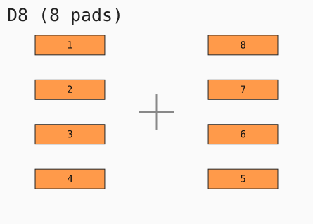
LM358DSOIC-8D8 / D8-L / D8-MSanity baseline. 8 horizontal pads, rot=0 throughout.
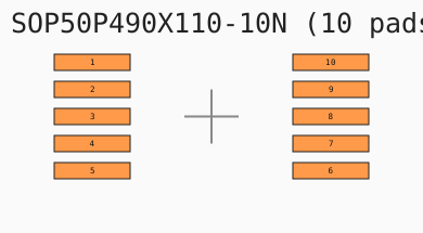
INA226AIDGSRVSSOP-10SOP50P490X110-10Nv3 layout (Convention B). Triggers FAT overshoot quirk.
ADS1115IDGSRVSSOP-10DGS0010A_L / _M / _N3 alternate density variants.
DRV8316RRGFRVQFN-40RGF0040E-IPC_A / _B / _C / -MFGIPC variants are Convention A; MFG variant is Convention B + extra fiducials/test points.

Skill Source

Edit AI Skill
---
name: altium-pcblib
description: >
  Native Rust crate that parses Altium .PcbLib (and .IntLib) binary footprint
  libraries β€” OLE2 Compound File container with Altium's reverse-engineered
  binary record format inside. Emits KiCad-shaped pad JSON so chipsmith,
  concur, and any other Adom tool that needs to read Altium binary footprints
  pulls from one source of truth instead of re-implementing OLE2 walking +
  binary record decoding.
  Public Rust API: parse_altium_pcblib_path(&Path), parse_altium_pcblib_bytes(&[u8]),
  render_footprint_svg(&Value), render_all_footprints_svg(&Value).
  Bundled CLI: altium-pcblib-svg <path> [--all] [-o out.svg] β€” emits the
  authoritative parser-side SVG so a downstream renderer disagreeing with
  the SVG is provably the bug, not the parser.
  Source is private (github.com/adom-inc/altium-pcblib); depend via
  Cargo path in the same workspace, or git URL on a build container.
  Trigger words: altium pcblib, altium intlib, parse altium binary footprint,
  altium ole2, altium compound file, altium binary record, .PcbLib, .IntLib,
  altium pad parser, read altium footprint in rust, altium-pcblib, altium
  cross-source, footprint consensus altium, altium svg debug, altium-pcblib-svg,
  authoritative footprint render, debug altium footprint, why is my altium pad
  rotated wrong, altium rotation convention, altium fat overshoot, altium pcblib
  malformed fat, multi-variant altium footprint, MFG vs IPC variant, RGF0040E.
---

# altium-pcblib β€” Adom's shared Altium .PcbLib parser (Rust crate)

`altium-pcblib` is a private Adom Rust crate that reads Altium Designer's
binary footprint libraries (`.PcbLib`, and the PCB stream embedded in
`.IntLib`) and emits per-pad JSON shaped like KiCad's `parse_kicad_mod`
output. Used by `adom-chipsmith` (Tab 4 cross-source agreement) and
`concur` (cross-source consensus check) so neither has to re-implement
OLE2 / CFBF walking or Altium's reverse-engineered binary record format.

> **This is a skill, not a library page.** The wiki's `library` type means
> "EDA part bundle = symbol + footprint + 3D + variants + pad↔pin mapping".
> `altium-pcblib` is a Rust crate, so it lives as a skill that points at the
> private GH repo. See `adom-wiki` skill β†’ "What each `<type>` means in Adom".

## Where the source lives

- Private GitHub repo: <https://github.com/adom-inc/altium-pcblib>
- Local workspace path (Adom container): `/home/adom/project/altium-pcblib`
- Cargo description (matches what's in `Cargo.toml`):
  > "Native Rust parser for Altium .PcbLib (and .IntLib) footprint libraries β€” extracts pads as KiCad-shaped JSON"

## Depending on it from another Adom Rust tool

In the workspace (chipsmith, concur, anything else under `/home/adom/project/`):

```toml
[dependencies]
altium-pcblib = { path = "../altium-pcblib" }
```

On a build container that doesn't have the workspace checkout:

```toml
[dependencies]
altium-pcblib = { git = "https://github.com/adom-inc/altium-pcblib", branch = "main" }
```

Single direct dep (`cfb`, the OLE2 reader) plus `anyhow` and `serde_json`.

## Public Rust API

```rust
// Parse from a file on disk.
pub fn parse_altium_pcblib_path(path: &Path) -> anyhow::Result<serde_json::Value>;

// Parse from raw bytes (handy for include_bytes! tests and HTTP bodies).
pub fn parse_altium_pcblib_bytes(bytes: &[u8]) -> anyhow::Result<serde_json::Value>;

// Render the parser's view of the footprint as standalone SVG. THIS IS THE
// AUTHORITATIVE GROUND TRUTH β€” if a downstream tool draws something different,
// the downstream tool is the bug.
pub fn render_footprint_svg(footprint: &serde_json::Value) -> String;

// Render primary + every alternate variant, stacked vertically in one SVG.
pub fn render_all_footprints_svg(parsed: &serde_json::Value) -> String;
```

The returned `Value` is shaped exactly like
`adom-chipsmith::view_library::parse_kicad_mod_text` output:

```json
{
  "module_name": "D8",
  "pad_count": 8,
  "pads": [{
    "number": "1", "type": "smd", "shape": "rect",
    "at": [-2.4638, -1.905, 0.0],
    "size": [1.9812, 0.5588],
    "layers": ["F.Cu", "F.Paste", "F.Mask"],
    "drill": null
  }],
  "silk_markers": [],
  "pin1_silk": { "found": false },
  "_source": "altium_pcblib",
  "_alternates": [ /* other footprints in the lib, sorted by pad_count desc */ ]
}
```

## CLI bin: `altium-pcblib-svg`

Single binary that ships with the crate. Use it any time you suspect a
downstream renderer is drawing pads wrong:

```bash
# Primary footprint, SVG to stdout.
altium-pcblib-svg /path/to/Foo.PcbLib > foo.svg

# Primary + every alternate variant stacked vertically.
altium-pcblib-svg /path/to/Foo.PcbLib --all -o foo-all.svg
```

Conventions baked into the SVG:

- 1 SVG unit = 1 mm. Open it in any browser at 50 px/mm by default.
- Y-down (matches both KiCad and our emitted JSON). Altium's Y-up is flipped at parse time.
- Rotation applied via `transform="rotate(deg cx cy)"` clockwise on screen β€” same direction KiCad displays.
- Pad numbers stay un-rotated for readability regardless of pad rotation.
- F.Cu pads = orange. B.Cu pads = blue. Thru-hole = green. Drill holes = white circle on top.
- Origin crosshair at (0, 0) with 1 mm arms β€” sanity-check pad placement.
- Footprint name + pad count in the top-left corner.

## Integration patterns

### chipsmith Tab 4 β€” cross-source agreement matrix

`adom-chipsmith/src/cli/view_library.rs` calls into the parser when it sees a
`<MPN>.PcbLib` sibling next to the `.kicad_mod`:

```rust
let altium_pcblib = args.dir.join(format!("{mpn}.PcbLib"));
if altium_pcblib.exists() && !sources.contains_key("altium") {
    match altium_pcblib::parse_altium_pcblib_path(&altium_pcblib) {
        Ok(parsed) => sources.insert("altium".to_string(), parsed),
        Err(e) => err(format!("altium parse failed: {e}")),
    }
}
```

The result drops straight into the same map that holds the KiCad / Fusion /
Datasheet entries, so the Tab 4 matrix lights up a fourth column with no
adapter needed. Alternates ride along under `_alternates` so the UI can
offer a variant picker.

### concur β€” adapter to lean Part shape

`concur/src/parsers/altium.rs` adapts the rich pad JSON down to concur's
lean `Part` shape (concur cares about pad designators + module name only):

```rust
pub fn parse(path: &Path) -> Result<Part> {
    let parsed = altium_pcblib::parse_altium_pcblib_path(path)?;
    let module_name = parsed.get("module_name").and_then(|v| v.as_str()).map(String::from);
    let pads: Vec<Pad> = parsed.get("pads").and_then(|v| v.as_array()).map(|arr| {
        arr.iter()
            .filter_map(|p| p.get("number").and_then(|v| v.as_str()).map(String::from))
            .map(|number| Pad { number })
            .collect()
    }).unwrap_or_default();
    Ok(Part {
        source: "altium".into(),
        source_part_name: module_name.clone(),
        pads,
        pins: Vec::new(),
        package: module_name.map(|raw_name| PackageInfo { raw_name, body_x_mm: None, body_y_mm: None }),
    })
}
```

For multi-variant `.PcbLib`s (DRV8316RRGFR has IPC_A / IPC_B / IPC_C / MFG),
concur's `parse_with_consensus_hint` walks primary + every alternate and picks
the variant whose pad count is closest to what the other parsed sources agree
on, then tiebreaks against names containing `MFG` / `DEBUG` / `TEST` / `FIDUCIAL`
(manufacturing layouts with extra non-pinout pads).

## Format quirks worth knowing

These are the things that bit us during reverse-engineering β€” they're
encoded in the parser, but if you extend it or debug a weird chip, here's
what's going on.

### 1. Some Altium .PcbLibs have FAT overshoot

INA226AIDGSR's PcbLib declares 256 FAT entries but only has 213 sectors.
The `cfb` crate refuses with `Malformed FAT … FAT has N entries, but file
has only M sectors`. The fix the parser uses: pad the input bytes to 1 MiB
with `0xFF` (CFBF "free sector" sentinel) before opening. The unreferenced
trailing sectors don't hold real data, so this is safe.

### 2. Per-record-type sub-block count

Altium records aren't uniform `[type][len][payload]`. Different record
types carry different numbers of `[u32 len][bytes]` sub-blocks:

- Pad (0x02): **6** sub-blocks (designator, layer-name pstring, four metadata blocks).
- Text (0x05): **2** sub-blocks (main + style trailer).
- Track / Arc / Via / Fill / Region / ComponentBody: **1** sub-block.

If you hit an unknown type byte mid-stream, the parser stops walking
gracefully β€” pads always come first, so by then we already have what we need.

### 3. Pad block-5 layout (the 194-byte v3 / 202-byte v4 pad data)

```
[0]      u8 layer (1 = TOP_CU, 32 = BOTTOM_CU, 21 = TOP_OVERLAY, ...)
[1]      u8 net/flag (0x08 in v3, 0x0c in v4 β€” version probe)
[2]      u8 reserved
[3..13]  10 bytes of 0xFF (component / net id sentinels)
[13..17] i32 LE x position (units = 1 / 10000 mil = 2.54e-6 mm)
[17..21] i32 LE y position (Altium Y-up β€” flipped to KiCad Y-down at parse)
[21..29] u32 LE x size, y size β€” top layer
[29..37] u32 LE x size, y size β€” mid layer (multi-layer thru-hole pads)
[37..45] u32 LE x size, y size β€” bottom layer
[45..49] u32 LE hole size (0 β†’ SMD; > 0 β†’ thru-hole)
[49..52] u8 Γ— 3 shape codes (1 round, 2 rect, 3 octagonal, 9 rounded-rect)
[52..60] f64 LE rotation in degrees β€” ONLY in 202-byte v4 layout
```

Past offset 60 the layout drifts between Altium releases (paste / mask
offsets, plated bool, GUIDs, primitive index). The parser stops at 60.

### 4. Two equally valid rotation conventions in the wild

This is the one that *looks* like a parser bug but isn't. Altium gives
library authors freedom in how to encode a rotated pad:

- **Convention A (matches KiCad):** store the pad as a "vertical stick"
  (xsize < ysize), set rotation = 90Β° on the side pads. DRV8316's IPC_A
  variant uses this.
- **Convention B (post-rotation):** store the physical post-rotation
  dimensions (xsize > ysize for a horizontal pad), set rotation = 0.
  DRV8316's MFG variant + INA226's v3 layout both use this.

Both render to the same physical pad on the PCB. A downstream tool that
compares `size[]` element-wise without applying rotation will see a 90Β°
mismatch in convention B β†’ KiCad. The fix lives in the consumer (compute
the post-rotation bbox before comparing), **not** in this parser.

When in doubt about whether your downstream is the bug, run
`altium-pcblib-svg` on the file β€” that's the parser's authoritative view.

### 5. Y-axis flip

Altium Y-up vs KiCad Y-down. The parser flips Y at parse time so emitted
`at[1]` is in KiCad convention. **Do not flip again downstream.**

### 6. Round shape with unequal w/h β†’ "oval"

KiCad's `circle` implies w == h. Altium's "round" (shape byte 1) covers
both true circles and stadium-shaped SMD pads with rounded ends. The
parser specializes: shape 1 with `(xsize - ysize).abs() < 1e-3` β†’ `circle`,
otherwise β†’ `oval` (KiCad's stadium).

## Visual proof β€” what "right" looks like

The crate ships three reference SVGs from the test corpus, generated by
`altium-pcblib-svg` (and reproducible any time):

- `playbooks/lm358d-soic8.svg` β€” SOIC-8 with 8 horizontal pads, two
  columns, rot=0 throughout. Sanity baseline.
- `playbooks/ina226-vssop10.svg` β€” VSSOP-10 v3 layout. xsize=1.4 mm,
  ysize=0.3 mm, rot=0 (Convention B above). Same physical pad as KiCad's
  rot=90 + size (0.3, 1.4) encoding.
- `playbooks/drv8316-all-variants.svg` β€” DRV8316RRGFR rendered with
  `--all`, showing the 41-pad IPC_A / IPC_B / IPC_C variants and the
  57-pad MFG variant stacked. The IPC variants match KiCad pin-for-pin
  (Convention A); MFG has extra fiducials, test points, and EP heatsink
  vias that don't appear in the chip's electrical pinout.

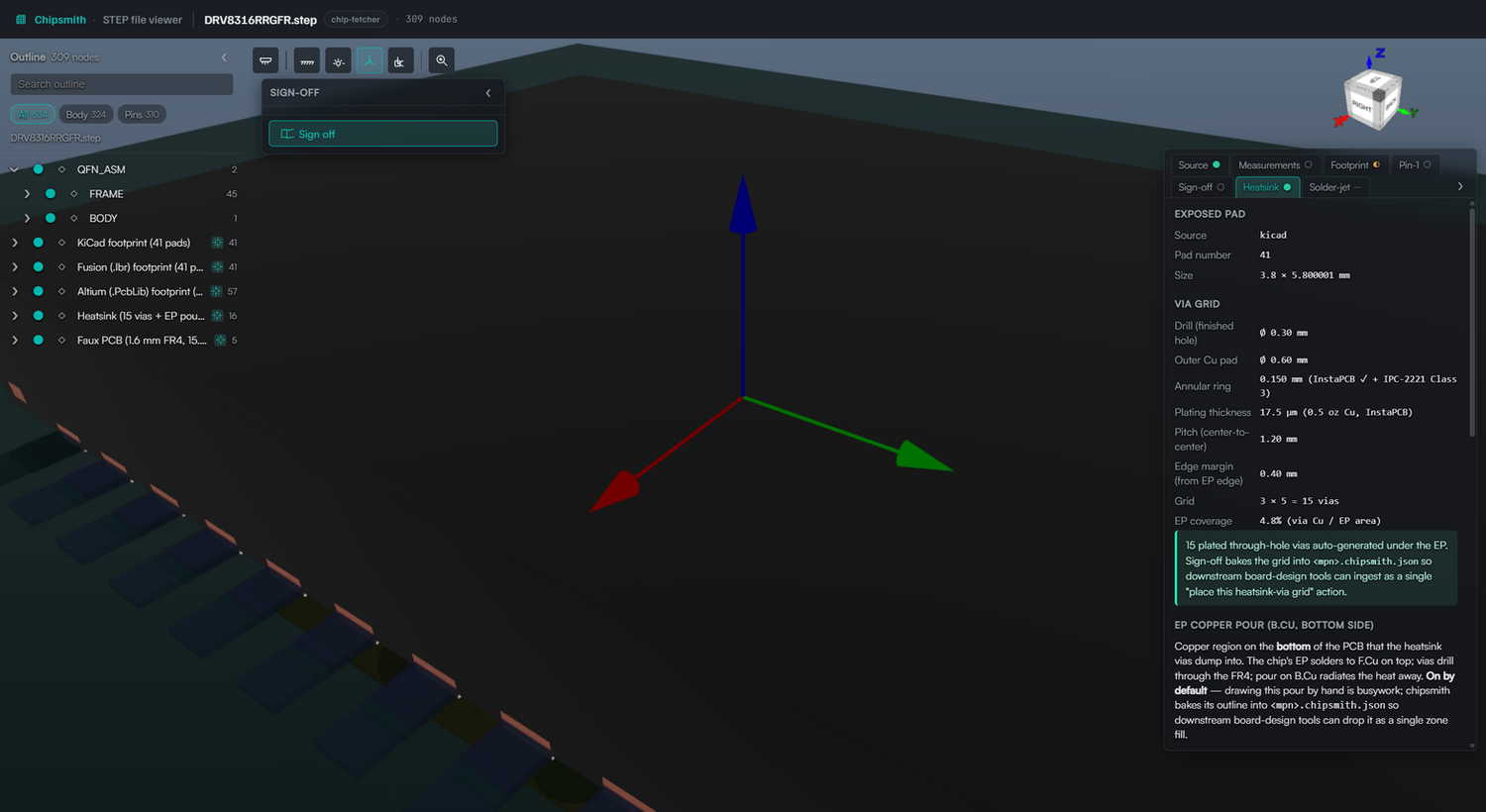
### chipsmith integration screenshot β€” DRV8316 in the 3D viewer

When the parser feeds chipsmith Tab 4, the Altium footprint appears as a
first-class Outline citizen alongside the KiCad and Fusion footprints. The
chipsmith view of `DRV8316RRGFR.step` shows:

- **Outline panel:** `KiCad footprint (41 pads)`, `Fusion (.lbr) footprint
  (41 pads)`, `Altium (.PcbLib) footprint (57)` β€” selected, drawing
  the MFG variant β€” plus `Heatsink (15 vias + EP pour)` and `Faux PCB
  (1.6 mm FR4)`.
- **3D canvas:** the full QFN-40 chip body with all 40 perimeter pads in
  their correct positions, the EP centred under the body, and the heatsink
  via grid drilled through the 1.6 mm FR4 plate. Tooltip on the FR4 plate
  shows `size 15.40 Γ— 1.60 Γ— 17.05 mm`.

The visual confirms three things at once: pads land in the right spots,
the multi-variant picker surfaces all four package options, and the
overlay layers stack correctly in the chipsmith Outline.

## Trouble-shooting checklist when a downstream renders pads wrong

1. **Run the authoritative SVG first.** `altium-pcblib-svg <path>.PcbLib > /tmp/auth.svg`. If pads are right in the SVG, the bug is downstream β€” not in this crate.
2. **Check which variant got picked.** `parsed.module_name` plus `_alternates[*].module_name`. Manufacturing variants often have extra pads vs the IPC pinout variant; concur uses `parse_with_consensus_hint` to pick the right one.
3. **Check rotation convention.** If pad 1 looks correct but pad 13 looks rotated 90Β° wrong, you're probably hitting Convention B vs A (see Format quirks #4) β€” your downstream is comparing or rendering size literally without applying rotation.
4. **Check Y direction.** If pads are mirrored top-to-bottom, your downstream double-flipped Y. Parser already emits KiCad Y-down.
5. **Scale.** SVG units are mm. If the rendered size is off by 1000Γ—, the consumer is treating mm as Β΅m or similar.

## Adding a new chip to the test corpus

When a new Altium PcbLib comes through chip-fetcher and you want to add
it as a regression test:

1. Drop the `.PcbLib` next to the existing test inputs (or use
   `chip-fetcher/library/<MPN>/`).
2. Run `altium-pcblib-svg <path> -o /tmp/new-chip.svg` and eyeball it.
3. Compare to the chip's `.kicad_mod` (or vendor-published IPC drawing).
4. If correct, add an `include_bytes!` test in `src/lib.rs::tests` like
   `lm358d_decodes_eight_pads_pad1_at_top_left` β€” assert pad count + a
   couple of representative positions.

Sub-Skills
?
What are Sub-Skills?

Sub-skills are community-contributed AI skill extensions for this component. They teach AI assistants about specific tools, configurators, or workflows.

Examples:

  • A manufacturer’s configuration tool for a motor controller
  • A community-written design guide for an amplifier circuit
  • An automated test/validation script for a sensor module

How to add one: Click Add Sub-Skill, provide the URL to your skill and a brief description. Submissions are reviewed by the Adom team before going live.

No sub-skills yet. Be the first to contribute one!

Recent activity

7 commits
  • 🏷
    Release v1.0.1 John Lauer 20 days ago
    v1.0.1 β€” re-attach sample prompts that didn't take on initial publish
  • ⬆
    Asset uploaded John Lauer 20 days ago
    add reference SVG: lm358d-soic8
  • ⬆
    Asset uploaded John Lauer 20 days ago
    add reference SVG: ina226-vssop10
  • ⬆
    Asset uploaded John Lauer 20 days ago
    add reference SVG: drv8316-all-variants
  • ⬆
    Asset uploaded John Lauer 20 days ago
    add hero image
  • ✎
    Edit v1.0.0 John Lauer 20 days ago
    add discovery_triggers + discovery_pitch
  • 🏷
    Release v1.0.0 John Lauer 20 days ago
    v1.0.0 β€” initial publish. Native Rust .PcbLib parser, SVG debug renderer, KiCad-shaped pad JSON. Used by chipsmith + concur.
0 revisions · Updated 2026-05-07 15:04:32