Paste this into Claude Code (VS Code panel, Adom editor, or terminal) to install:
Search the Adom Wiki for the molecule "RP2350A Mini Molecule" (slug: rp2350a-mini) at https://wiki-ufypy5dpx93o.adom.cloud/wiki/molecules/rp2350a-mini. Download its symbol (.kicad_sym), footprint (.kicad_mod), and 3D model (.glb/.step) assets into my current KiCad project under symbols/, footprints/, and 3dmodels/ directories. Register them in the project library tables. Show me the files once installed.
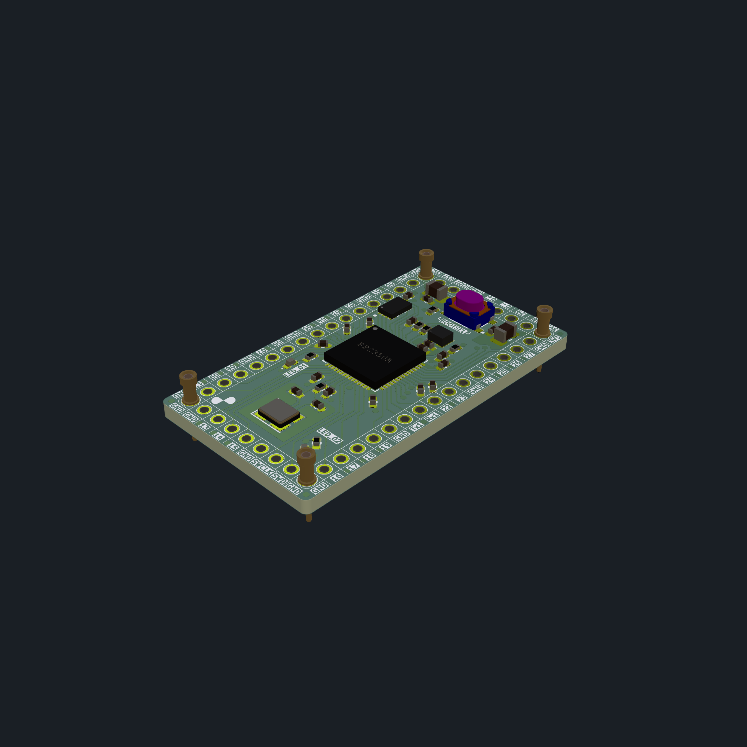
General-purpose RP2350A castellated module — 20×36 mm, dual-core Arm Cortex-M33 / Hazard3 RISC-V MCU with 16 Mbit QSPI flash, USB, UART, SWD debug, and 4 ADC channels. 26 user-programmable GPIO/ADC pins exposed on castellated machine contacts (44 total contacts + 4 corner machine pins). Drop-in MCU module for Adom workcell designs.
How It Works
The RP2350A Mini is a minimal breakout of the Raspberry Pi RP2350A — all user-accessible GPIOs, USB, UART, SWD, ADC, and power are routed to castellated machine contacts around the perimeter. It is designed to be soldered onto a carrier board as a sub-module (like the RP2040 PICAN), providing the MCU brain for any workcell molecule. Power comes in through the corner machine pins (+3V3 on MP1/MP4). The on-board buck converter generates the 1.1V core voltage from 3.3V.
Overview
| Property | Value |
|---|
| Molecule ID | rp2350a-mini |
| Board Size | 20.0 × 36.0 mm |
| MCU | RP2350A (QFN-60) — dual-core Cortex-M33 + Hazard3 RISC-V, 150 MHz |
| Flash | W25Q16JVUXIQ — 16 Mbit (2 MB) QSPI |
| Crystal | 12 MHz (X322512MSB4SI) |
| Regulator | On-chip buck converter (3.3V → 1.1V core, external 3.3 µH inductor) |
| USB | USB 2.0 (D+/D- on machine contacts) |
| Machine Contacts | 44 contacts + 4 corner machine pins |
| KiCad Version | 7/8 |
Key ICs
| Ref | Part | Package | Function |
|---|
| U1 | RP2350A | QFN-60 | Dual-core MCU (Cortex-M33 + RISC-V) |
| U2 | W25Q16JVUXIQ | USON-8 | 2 MB QSPI flash |
Machine Contact Pin Mapping
4 corner machine pins + 44 castellated contacts on all 4 edges.
Corner Machine Pins
| Pin | Net | Function |
|---|
| MP1 | +3V3 | 3.3V power input |
| MP4 | +3V3 | 3.3V power input |
| MP2 | GND | Ground |
| MP3 | GND | Ground |
Left Edge (top to bottom)
| Contact | Net | Function |
|---|
| MC1 | GND | Ground |
| MC2 | GPIO0 | General purpose I/O |
| MC3 | GPIO1 | General purpose I/O |
| MC4 | GND | Ground |
| MC5 | GPIO2 | General purpose I/O |
| MC6 | GPIO3 | General purpose I/O |
| MC7 | GPIO4 | General purpose I/O |
| MC8 | GPIO5 | General purpose I/O |
| MC9 | GND | Ground |
| MC10 | GPIO6 | General purpose I/O |
| MC11 | GPIO7 | General purpose I/O |
| MC12 | GND | Ground |
| MC13 | GPIO8 | General purpose I/O |
| MC14 | GPIO9 | General purpose I/O |
| MC15 | GPIO12 | General purpose I/O |
Bottom Edge (left to right)
| Contact | Net | Function |
|---|
| MC16 | GND | Ground |
| MC17 | GPIO13 | General purpose I/O |
| MC18 | GPIO14 | General purpose I/O |
| MC19 | GPIO15 | General purpose I/O |
| MC20 | GND | Ground |
| MC21 | SWCLK | SWD debug clock |
| MC22 | SWD | SWD debug data |
Right Edge (bottom to top)
| Contact | Net | Function |
|---|
| MC23 | GPIO16 | General purpose I/O |
| MC24 | GPIO17 | General purpose I/O |
| MC25 | GPIO18 | General purpose I/O |
| MC26 | GPIO19 | General purpose I/O |
| MC27 | GND | Ground |
| MC28 | Tx1 | UART1 TX |
| MC29 | Rx1 | UART1 RX |
| MC30 | GPIO22 | General purpose I/O |
| MC31 | GPIO23 | General purpose I/O |
| MC32 | GND | Ground |
| MC33 | GPIO24 | General purpose I/O |
| MC34 | GPIO25 | General purpose I/O |
| MC35 | GPIO26 / ADC0 | ADC channel 0 |
| MC36 | GPIO27 / ADC1 | ADC channel 1 |
| MC37 | GND | Ground |
Top Edge (right to left)
| Contact | Net | Function |
|---|
| MC38 | GPIO28 / ADC2 | ADC channel 2 |
| MC39 | GPIO29 / ADC3 | ADC channel 3 |
| MC40 | USB_D- | USB data minus |
| MC41 | USB_D+ | USB data plus |
| MC42 | GND | Ground |
| MC43 | BOOT | Bootloader select |
| MC44 | RST | Reset |
GPIO Summary
| GPIO Range | Count | Available Functions |
|---|
| GPIO0–GPIO9 | 10 | SPI, I2C, UART, PWM, PIO |
| GPIO10–GPIO11 | 2 | (LED indicators, directly on module) |
| GPIO12–GPIO19 | 8 | SPI, I2C, UART, PWM, PIO, HSTX (up to 300 Mb/s) |
| GPIO22–GPIO25 | 4 | PWM, PIO |
| GPIO26–GPIO29 | 4 | ADC0–ADC3 (12-bit, 500 ksps) |
GPIO10 and GPIO11 are used on-board for status LEDs and are not routed to contacts.
Status LEDs
| LED | Color | Function |
|---|
| D1 | Red | Power indicator |
| D2 | Blue | User LED (GPIO11) |
Programming
- USB bootloader: Bridge BOOT (MC43) to GND and power cycle — RP2350 enters USB mass storage mode. Copy a
.uf2 file to flash.
- SWD debug: SWCLK (MC21) and SWD (MC22) on the bottom edge. Use with a PiProbe or any CMSIS-DAP adapter.
- picotool:
picotool load firmware.uf2 -f over USB or SWD.
Power
| Rail | Source | Notes |
|---|
| +3V3 | MP1/MP4 corner pins | External 3.3V supply required |
| +1V1 | On-chip buck (L1 = 3.3 µH) | RP2350 core voltage, auto-generated |
Fabrication
- BOM:
jlcpcb/production_files/BOM-Molecule_RP2350A_Mini.csv
- CPL:
jlcpcb/production_files/CPL-Molecule_RP2350A_Mini.csv
- Gerbers:
jlcpcb/production_files/GERBER-Molecule_RP2350A_Mini.zip
3D Models
Molecule_RP2350A_Mini.glb — assembled board GLBMolecule_RP2350A_Mini.step — STEP modelRP2350_QFN60.step — RP2350 IC STEP model
No sub-skills yet. Be the first to contribute one!