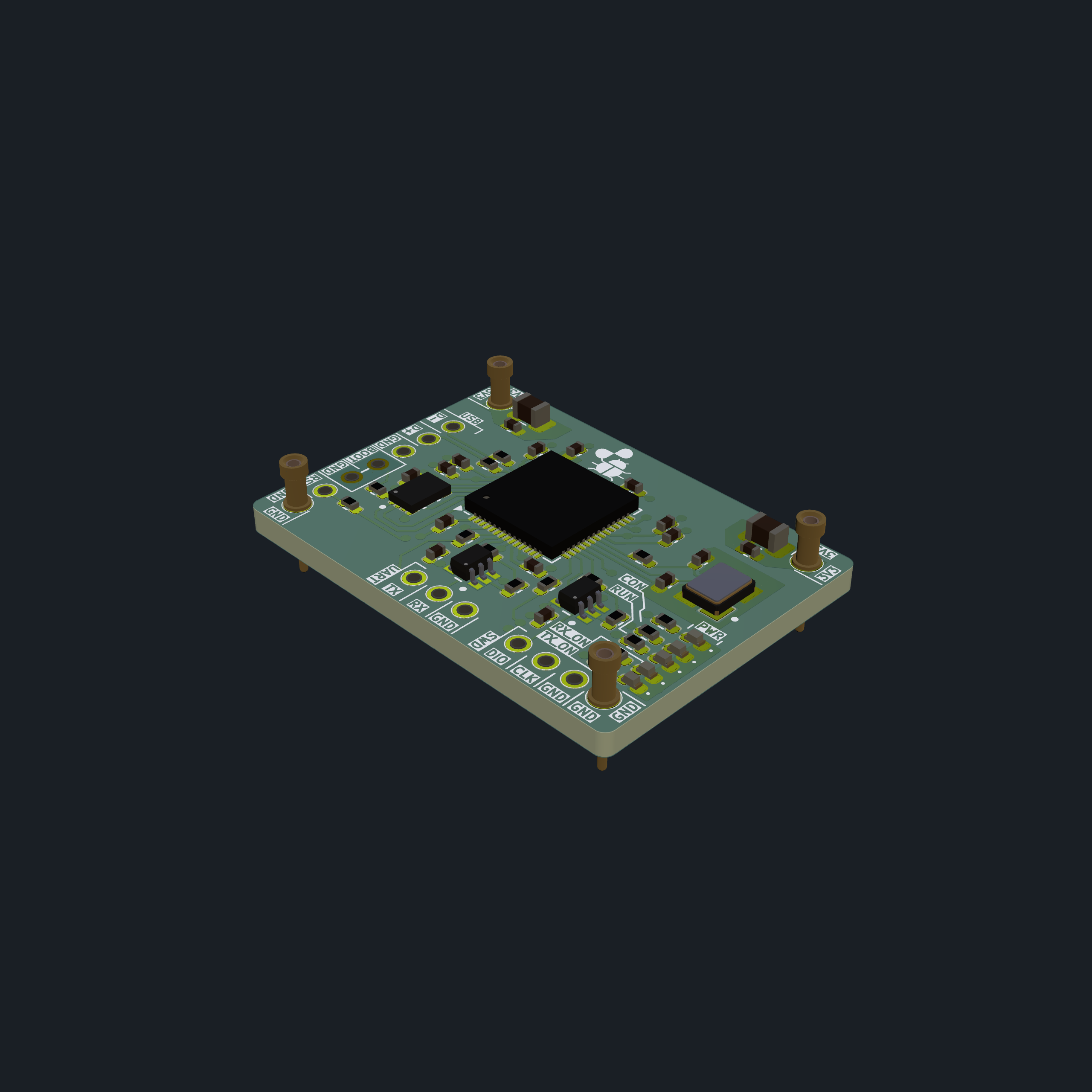
RP2040-based SWD debug probe molecule — 28×20 mm, runs the Raspberry Pi Debugprobe (picoprobe) firmware. Provides SWD debug (CLK + DIO) and UART passthrough (TX + RX) to target devices via machine contacts. USB connection for host interface. Used for programming and debugging RP2040/RP2350 and other Arm targets in the Adom workcell.
How It Works
This board is designed around and runs the official Raspberry Pi debugprobe.uf2 firmware (raspberrypi/debugprobe). The hardware pin assignments, USB descriptor configuration, and level-shifted SWD/UART interfaces are all matched to the debugprobe firmware's expected GPIO mapping — it is a drop-in compatible debug probe that presents as a CMSIS-DAP device over USB.
The PiProbe connects to a host PC via USB (D+/D- on machine contacts MC1/MC2). The host runs OpenOCD, probe-rs, or the Raspberry Pi Debug Probe extension to flash and debug a target MCU. SWD signals (CLK/DIO) and UART (TX/RX) are routed out through machine contacts on the bottom edge, connecting to the target molecule in the workcell. Power comes in through the machine pins (+3V3 on MP1/MP4), not from the USB host.
Overview
| Property | Value |
|---|---|
| Molecule ID | piprobe-molecule-v1-2 |
| Board Size | 28.0 × 20.0 mm |
| MCU | RP2040 (QFN-56) |
| Flash | W25Q16JVUXIQ — 16 Mbit (2 MB) QSPI |
| Level Shifters | 2× 74AUP1T17GW — SWD signal conditioning |
| Crystal | 12 MHz |
| Firmware | Raspberry Pi Debugprobe (picoprobe) |
| Machine Contacts | 9 contacts + 4 corner machine pins |
| KiCad Version | 7/8 |
Key ICs
| Ref | Part | Package | Function |
|---|---|---|---|
| U1 | RP2040 | QFN-56 | Debug probe MCU |
| U2 | W25Q16JVUXIQ | USON-8 | 2 MB QSPI flash (firmware storage) |
| U3 | 74AUP1T17GW | SC-70-5 | SWD DIO level shifter / buffer |
| U4 | 74AUP1T17GW | SC-70-5 | SWD CLK level shifter / buffer |
Machine Contact Pin Mapping
Corner Machine Pins
| Pin | Position | Net | Function |
|---|---|---|---|
| MP1 | Top-left | +3V3 | 3.3V power input |
| MP4 | Top-right | +3V3 | 3.3V power input |
| MP2 | Bottom-left | GND | Ground |
| MP3 | Bottom-right | GND | Ground |
Left Edge — USB & Control
| Contact | Net | Function |
|---|---|---|
| MC1 | USB_D- | USB data minus (to host) |
| MC2 | USB_D+ | USB data plus (to host) |
| MC3 | GND | Ground |
| MC5 | RST | Target reset |
| JP1 | BOOTSEL / GND | Boot select jumper (bridge to enter USB bootloader) |
Bottom Edge — Debug & UART (to target)
| Contact | Net | Function |
|---|---|---|
| MC6 | TX | UART TX (probe → target RX) |
| MC7 | RX | UART RX (target TX → probe) |
| MC8 | GND | Ground |
| MC9 | GND | Ground |
| MC10 | DIO | SWD data (bidirectional) |
| MC11 | CLK | SWD clock |
Status LEDs
| LED | Color | Function |
|---|---|---|
| D1 | Red | Power indicator |
| D2 | Green | DAP connected |
| D3 | Yellow | UART TX activity |
| D4 | Yellow | UART RX activity |
| D5 | Green | Probe ready |
SWD Signal Path
The SWD signals are buffered through 74AUP1T17GW level shifters (U3, U4) with 100 Ω series resistors for signal integrity. This provides clean edges and protects the RP2040 GPIOs from target-side transients.
RP2040 GPIO → 100Ω → 74AUP1T17GW → MC10 (DIO) / MC11 (CLK) → Target
Firmware
The probe runs the official Raspberry Pi Debugprobe (picoprobe) firmware. To flash:
- Bridge JP1 (BOOTSEL) and power cycle — RP2040 enters USB mass storage mode
- Copy the
.uf2firmware file to the mounted drive - Remove JP1 bridge — probe boots into debugprobe mode
Programming a Target
From the host (or this container via USB passthrough):
# OpenOCD
openocd -f interface/cmsis-dap.cfg -f target/rp2040.cfg -c "program firmware.elf verify reset exit"

# picotool (over SWD via the probe)
picotool load firmware.uf2 -f

# probe-rs
probe-rs run --chip RP2040 firmware.elf
Fabrication
KiCad project files included in the source bundle.