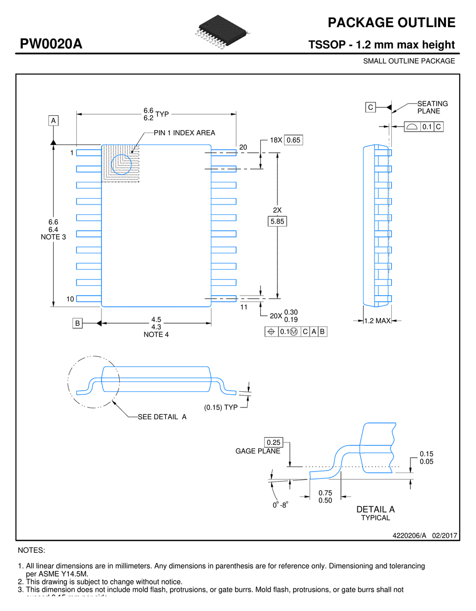
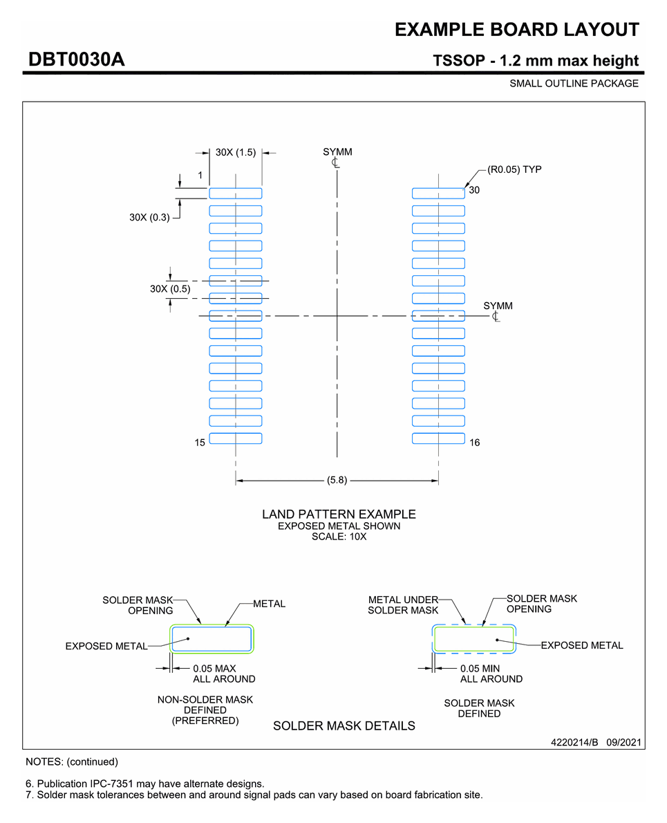
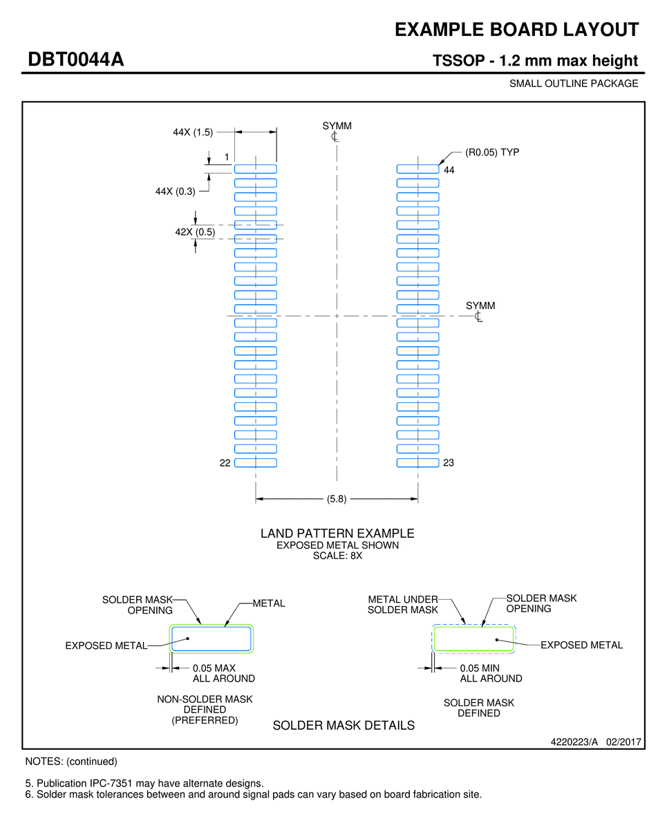

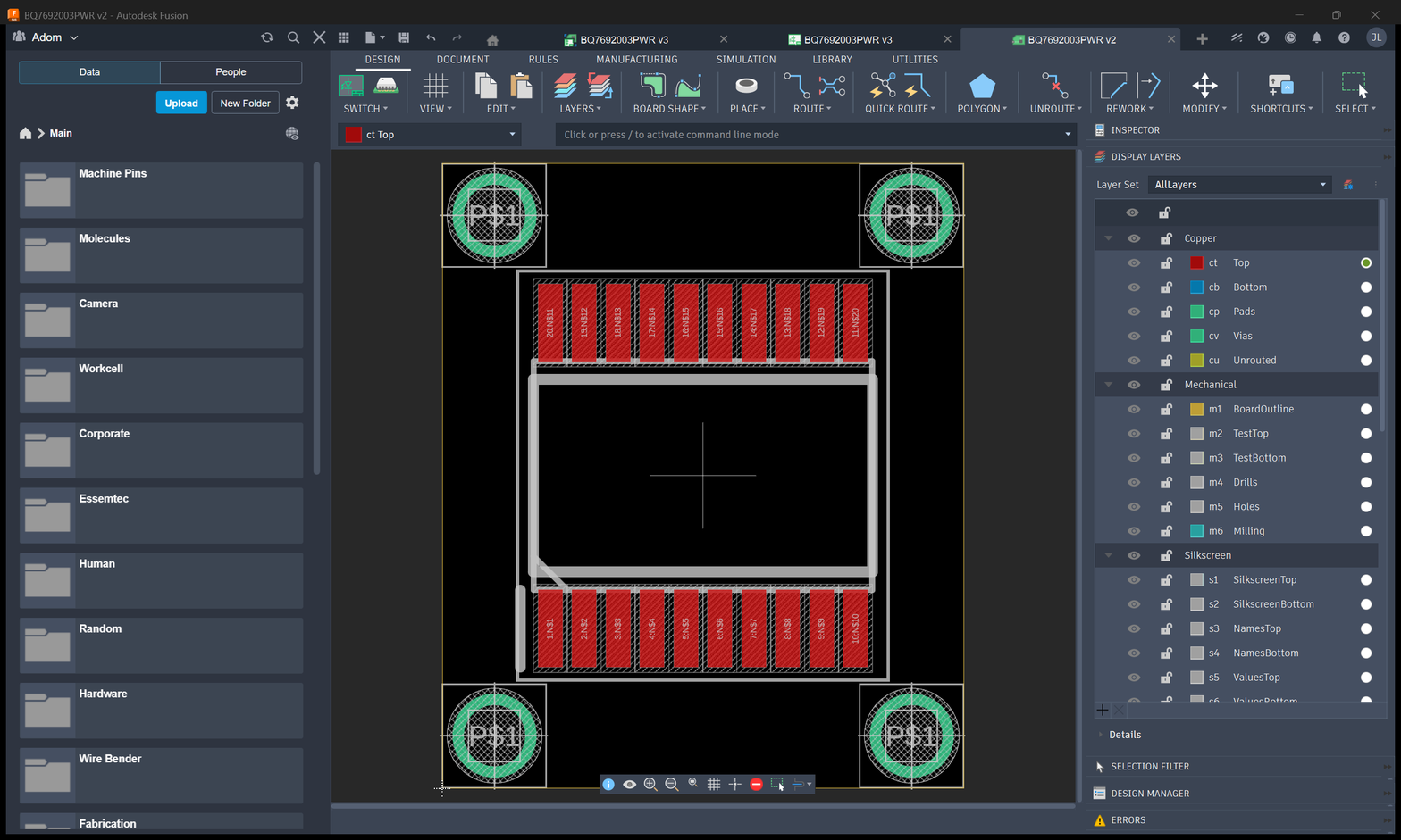





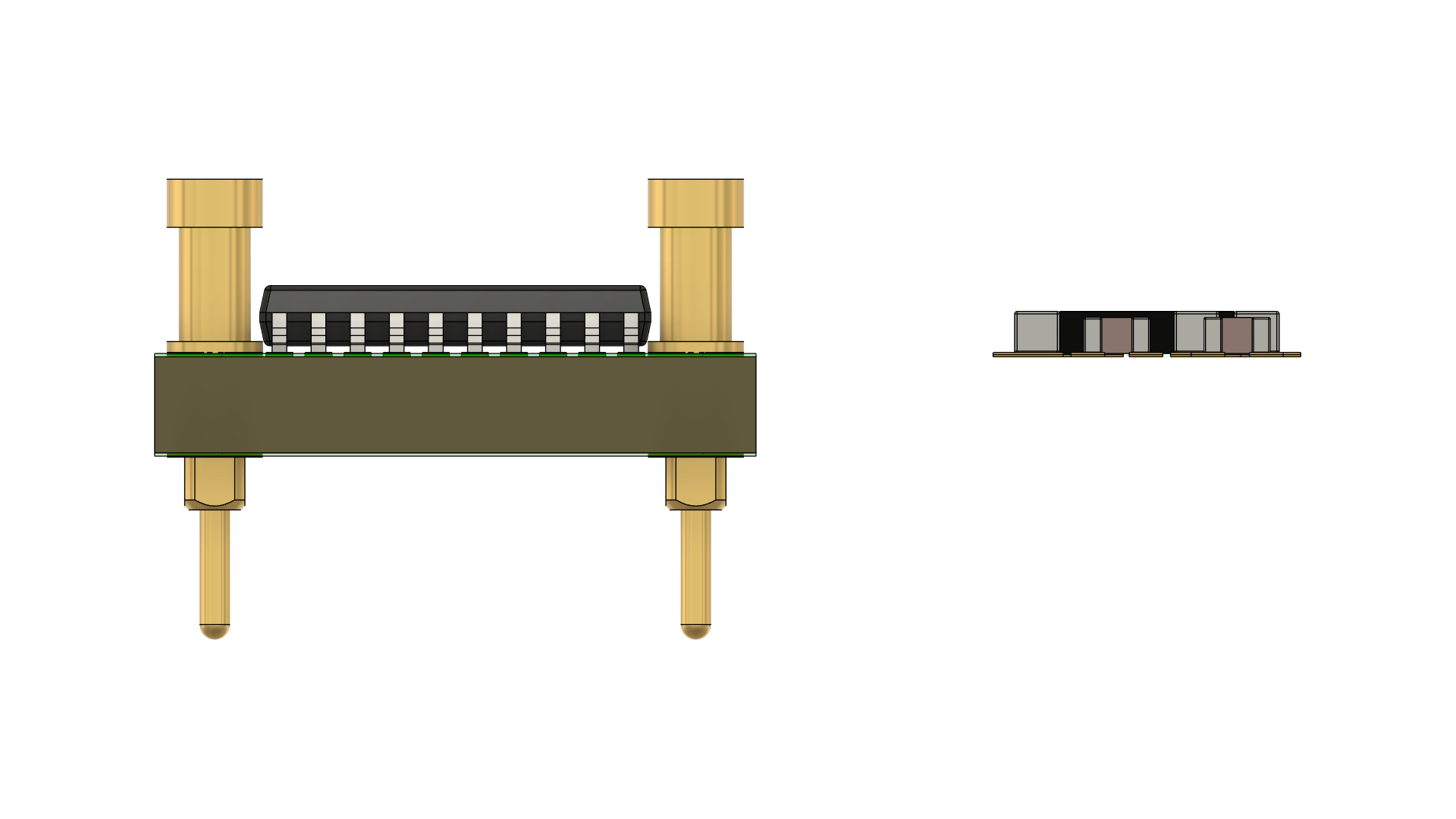
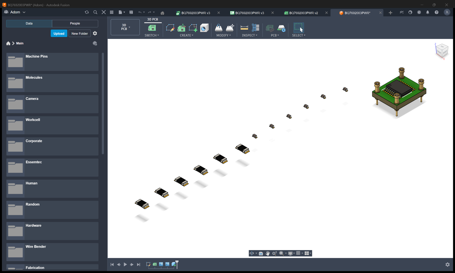
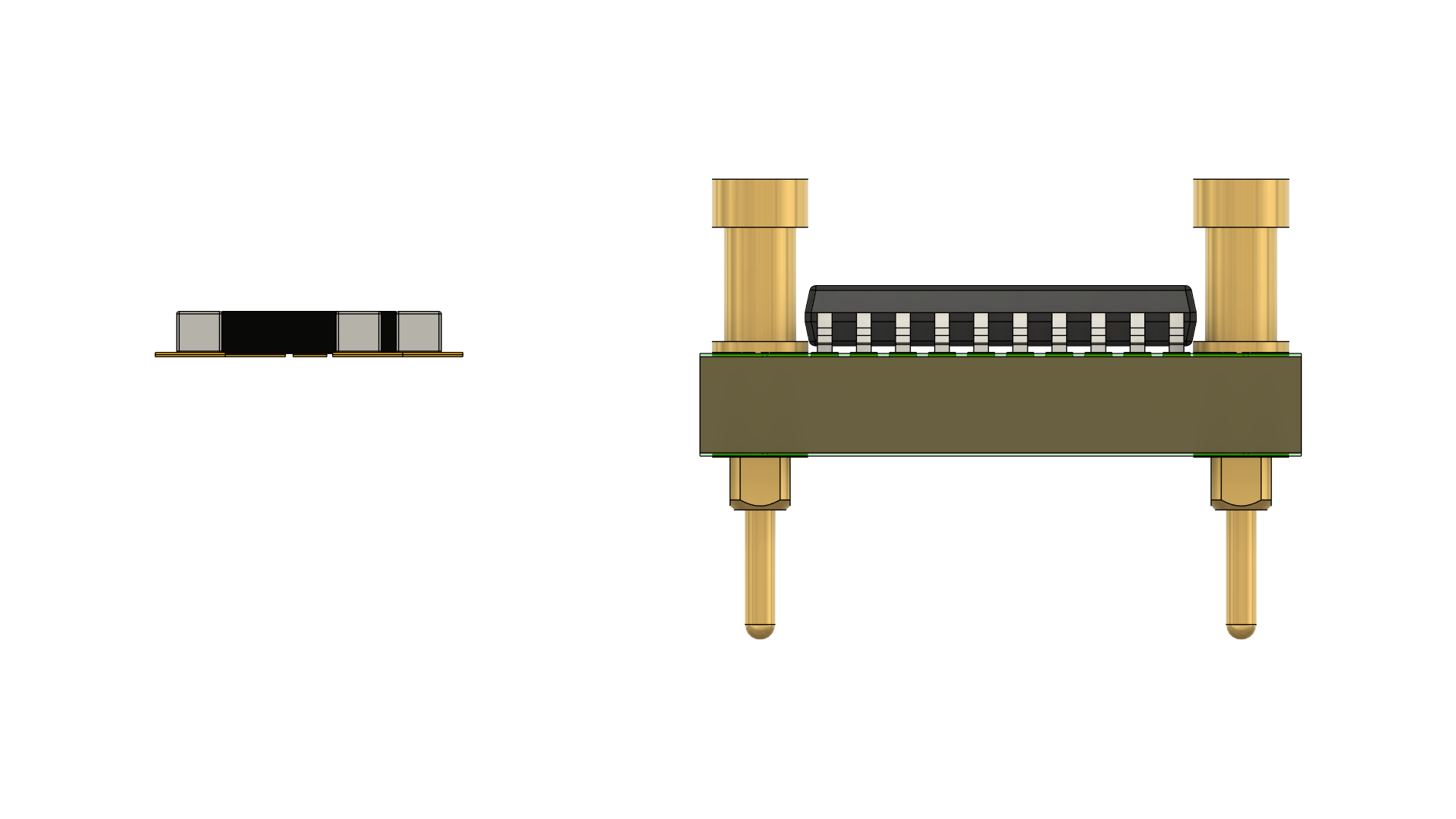
Source: Texas Instruments — BQ769x0 3-Series to 15-Series Cell Battery Monitor Family (SLUSBK2I) Manufacturer: Texas Instruments Part Number: BQ7692003PWR Family: BQ76920 / BQ76930 / BQ76940 Document: SLUSBK2I — October 2013, Revised March 2022 (67 pages) Package: 20-TSSOP (PW), 6.5 mm × 4.4 mm × 1.2 mm I²C Address: 0x08 (7-bit) LDO: 3.3 V CRC: Yes
Description
The BQ7692003PWR is a factory-preconfigured orderable variant of the Texas Instruments BQ76920, a 3-to-5-series-cell analog front-end (AFE) for lithium-ion and lithium-iron-phosphate battery pack monitoring and protection. It is part of the broader BQ769x0 family — BQ76920 (3–5 cells, 20-TSSOP), BQ76930 (6–10 cells, 30-TSSOP), and BQ76940 (9–15 cells, 44-TSSOP) — all sharing the same register map and digital interface.
The BQ7692003PWR variant is factory-programmed with I²C address 0x08, a 3.3 V REGOUT LDO, and I²C CRC enabled, shipped in tape-and-reel. No EEPROM programming is required.
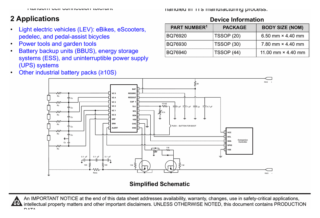
Typical applications include light electric vehicles (eBikes, eScooters, pedelecs), power tools and garden tools, battery backup units (BBU), energy storage systems (ESS), UPS systems, and other ≥10-cell industrial battery packs (where a BQ76940 would be the right family member).
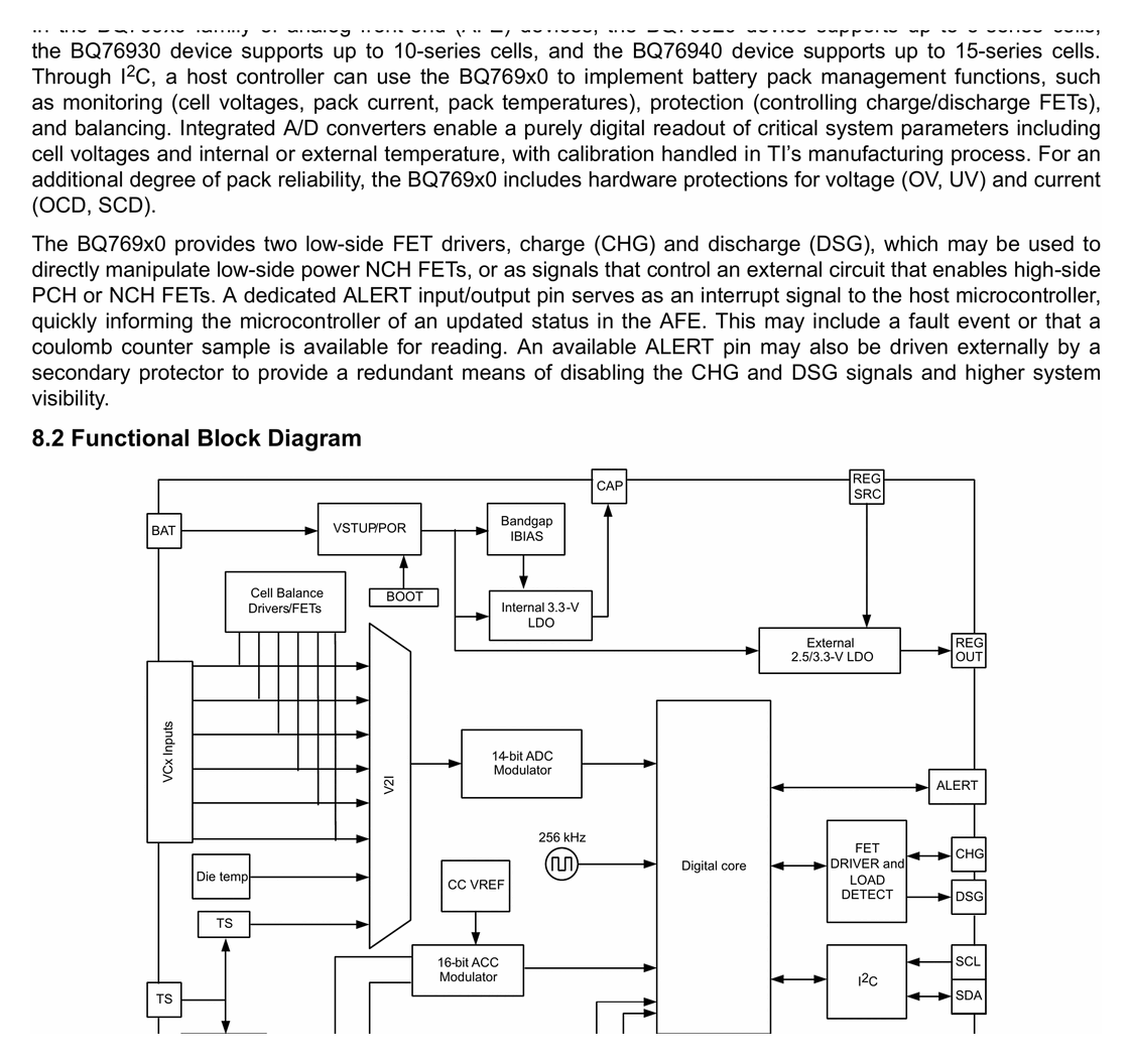
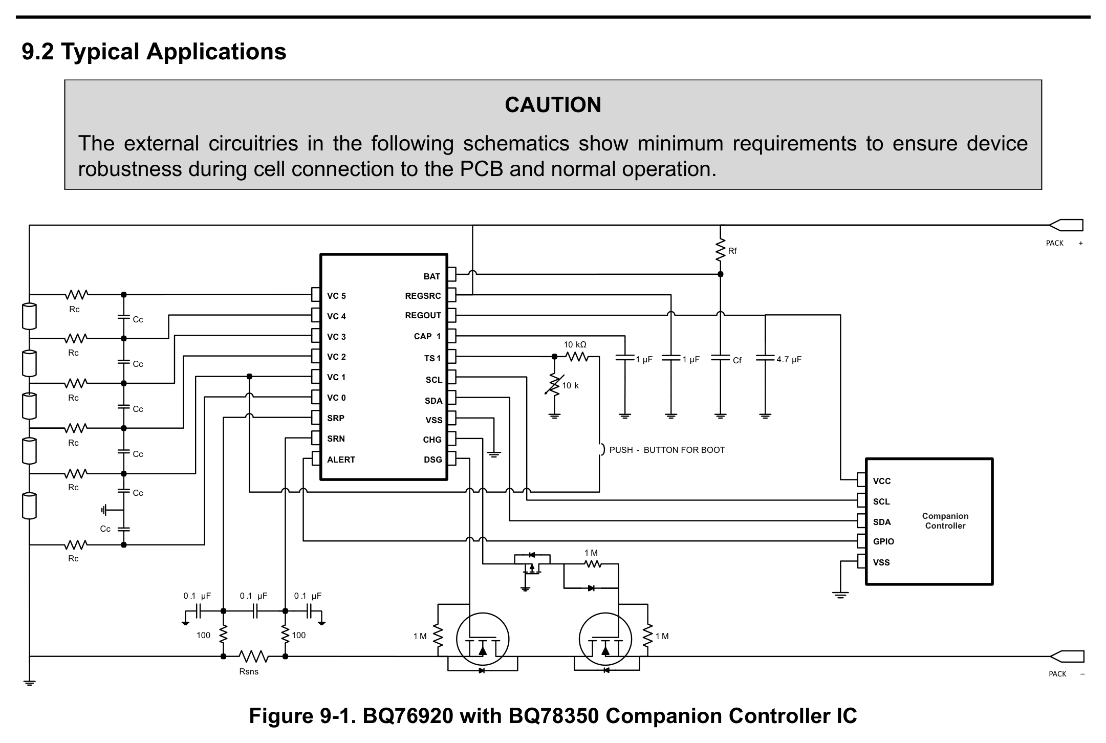
The device integrates cell voltage measurement, pack current measurement (coulomb counter), internal die temperature plus up to three external thermistor inputs, hardware overcurrent / short-circuit / overvoltage / undervoltage protection with configurable thresholds, charge and discharge low-side NCH FET drivers, and cell balancing FETs. A host microcontroller drives the pack-management logic over I²C; an ALERT interrupt line signals protection events and ADC-ready conditions.
Key Specifications
| Parameter | Value |
|---|---|
| Cells Supported | 3 to 5 (BQ76920 family) |
| Supply Voltage (V_BAT) | 6 V to 25 V |
| Absolute Max Supply | 36 V (BQ76920); up to 108 V per-pin rating within family |
| LDO Output (REGOUT) | 3.3 V |
| I²C Address | 0x08 (7-bit) |
| I²C CRC | Enabled |
| I²C Clock Frequency | up to 100 kHz |
| Cell ADC Resolution | 14-bit |
| Cell ADC LSB | 382 µV |
| Coulomb Counter ADC | 16-bit, 8.44 µV LSB |
| Thermistor Inputs | 3 (103AT) |
| Protection Hardware | OV, UV, OCD, SCD |
| Cell Balancing | Integrated FETs per cell |
| FET Drivers | Low-side NCH CHG + DSG |
| Package | 20-TSSOP (PW), 6.5 × 4.4 × 1.2 mm |
| Operating Temperature | −40 °C to +85 °C |
| Startup Current (SHIP mode) | 0.6 µA typ |
Features
- Analog front-end for 3-to-5-series Li-ion / LiFePO₄ battery packs
- Pure digital interface (I²C with optional CRC)
- 14-bit internal ADC for cell voltage, die temperature, and external thermistor
- Separate 16-bit coulomb-counter ADC for pack current
- Direct support for up to three 103AT thermistors
- Hardware overcurrent in discharge (OCD), short-circuit in discharge (SCD), overvoltage (OV), and undervoltage (UV) protections
- Secondary-protector fault detection input
- Integrated cell-balancing FETs (one per cell)
- Low-side NCH CHG and DSG FET drivers
- Alert interrupt line to host MCU (ALERT pin, open-drain)
- 3.3 V REGOUT LDO with external pass FET option (REGSRC)
- No EEPROM programming required — device is factory-preconfigured
- High-voltage absolute-maximum supply rating (up to 108 V, family-dependent)
- Random cell-connection order tolerant during pack assembly
- SHIP mode for ultra-low-power storage (0.6 µA typical)
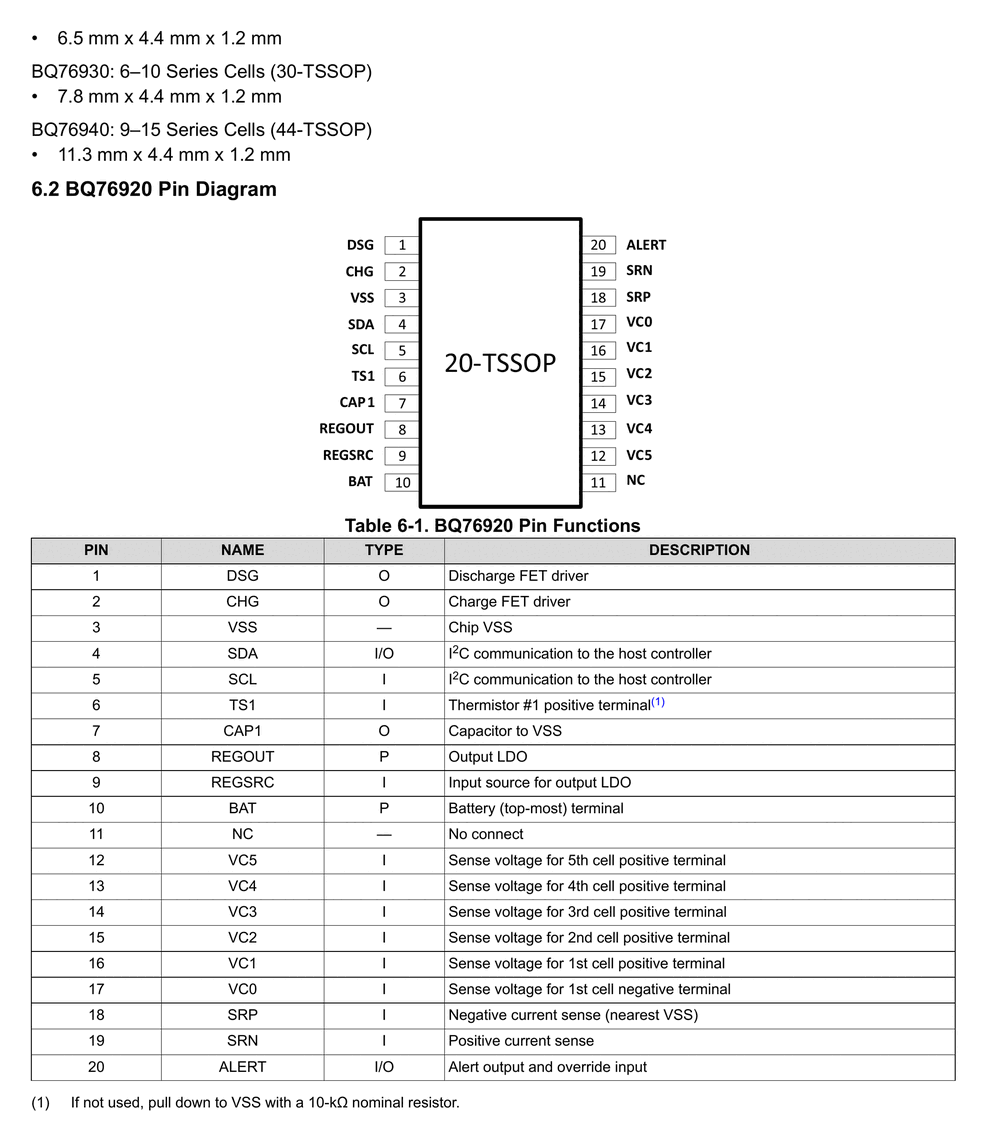
Pin Configuration
| Pin | Name | Type | Description |
|---|---|---|---|
| 1 | DSG | O | Discharge FET driver (low-side NCH) |
| 2 | CHG | O | Charge FET driver (low-side NCH) |
| 3 | VSS | — | Chip VSS / device ground |
| 4 | SDA | I/O | I²C data |
| 5 | SCL | I | I²C clock |
| 6 | TS1 | I | Thermistor #1 positive terminal (pull to VSS via 10 kΩ if unused) |
| 7 | CAP1 | O | Capacitor to VSS (internal bias decoupling) |
| 8 | REGOUT | P | Output LDO (3.3 V in this variant) |
| 9 | REGSRC | I | Input source for output LDO |
| 10 | BAT | P | Battery top-most terminal (supply pin) |
| 11 | NC | — | No connect |
| 12 | VC5 | I | Sense voltage, 5th cell positive terminal |
| 13 | VC4 | I | Sense voltage, 4th cell positive terminal |
| 14 | VC3 | I | Sense voltage, 3rd cell positive terminal |
| 15 | VC2 | I | Sense voltage, 2nd cell positive terminal |
| 16 | VC1 | I | Sense voltage, 1st cell positive terminal |
| 17 | VC0 | I | Sense voltage, 1st cell negative terminal |
| 18 | SRP | I | Current-sense resistor, side nearest VSS |
| 19 | SRN | I | Current-sense resistor, positive side |
| 20 | ALERT | I/O | Alert output / override input (open-drain) |
Absolute Maximum Ratings
Over-operating free-air temperature range unless otherwise noted. Stresses beyond these ratings may cause permanent damage.
| Parameter | Min | Max | Unit |
|---|---|---|---|
| V_BAT (BAT − VSS) | −0.3 | 36 | V |
| V_I (VC0 − VSS) where n = 1..5 | −0.3 | (n × 7.2) | V |
| V_I (SRN, SRP, SCL, SDA) | −0.3 | 9 | V |
| V_I (VC0 − VC5x, CAP1 − VC5x, CAP1 − VSS, TS2 − VC5x, TS1 − VSS)² | −0.3 | 3.6 | V |
| V_I (REGSRC) | −0.3 | 36 | V |
| V_O (REGOUT, ALERT) | −0.3 | 36 | V |
| V_O (DSG) | −0.3 | 20 | V |
| V_O (CHG) | −0.3 | V_CHG,CLAMP | V |
| I_CB Cell-balancing current (per cell) | — | 70 | mA |
| I_DD Discharge pin input current when disabled | — | 7 | mA |
| T_stg Storage temperature | −65 | 150 | °C |
| T_SOL Lead temperature (soldering, 10 s) | — | 300 | °C |
Recommended Operating Conditions
Over-operating free-air temperature range unless otherwise noted. All voltages relative to VSS.
| Parameter | Min | Typ | Max | Unit |
|---|---|---|---|---|
| V_BAT Supply voltage (BAT − VSS) | 6 | — | 25 | V |
| V_BAT Cell-input differential (VC_n − VC_n−1) | 2 | — | 5 | V |
| V_IN (VC0 − VSS) | 0 | — | 5 × n | V |
| V_IN (TS1 − VSS) | −10 | — | 10 | mV |
| V_IN (SRN) | −200 | — | 200 | mV |
| V_OUT (CAP1 − VSS) | 0 | — | 3.6 | V |
| V_OUT (REGOUT) | 0 | — | 16 | V |
| I_CB Cell balancing current (internal per cell) | 0 | — | 50 | mA |
| R_C External cell filter resistance | 40 | 100 | 1 K | Ω |
| R_S Sense resistor filter resistance | 40 | 100 | 1 K | Ω |
| C_C External cell input capacitance | 0.1 | 1 | 10 | µF |
| C_T External supply filter capacitance | 40 | 100 | 1 K | µF |
| C_F External sense filter capacitance | 1 | 10 | 40 | µF |
| R_FILT Sense resistor filter resistance | 100 | 1 K | — | Ω |
| R_ALERT ALERT pin to VSS resistor | — | 1 M | — | Ω |
| C_L REGOUT loading capacitance | 1 | 4.7 | — | µF |
| C_CAP REGSRC, CAP1, CAP2 and CAP3 output capacitance | 1 | — | — | µF |
| R_TS External thermistor nominal resistance (103AT at 25 °C) | — | 10 K | — | Ω |
| T_OPR Operating free-air temperature | −40 | — | 85 | °C |
Electrical Characteristics
Typical conditions: T_A = 25 °C, BAT = 18 V (BQ76920) / 36 V (BQ76930) / 48 V (BQ76940), VCC = 4 V. Min/max apply over −40 °C to +85 °C unless noted.
Supply currents
| Parameter | Test Condition | Min | Typ | Max | Unit |
|---|---|---|---|---|---|
| I_DD Normal mode, ADC off, CC off | Sum of I_CC,BAT and I_CC,REGSRC | — | 40 | 60 | µA |
| I_DD Normal mode, ADC on, CC off | — | 60 | 90 | µA | |
| I_DD Normal mode, ADC off, CC on | — | 110 | 165 | µA | |
| I_DD Normal mode, ADC on, CC on | — | 130 | 195 | µA | |
| I_CC,BAT Normal mode, ADC off | Into BAT pin | — | 30 | 45 | µA |
| I_CC,BAT Normal mode, ADC on | — | 50 | 75 | µA | |
| I_CC,REGSRC Normal mode, CC off | Into REGSRC pin | — | 10 | 15 | µA |
| I_CC,REGSRC Normal mode, CC on | — | 80 | 120 | µA | |
| I_SHIP SHIP/SHUTDOWN mode | Device in full shutdown, only VSTUP/BG and BOOT detector on | — | 0.6 | 1.8 | µA |
Cell voltage measurement
| Parameter | Test Condition | Min | Typ | Max | Unit |
|---|---|---|---|---|---|
| ADC range | V_CELL measurements | 2 | — | 5 | V |
| ADC LSB value | — | 382 | — | µV | |
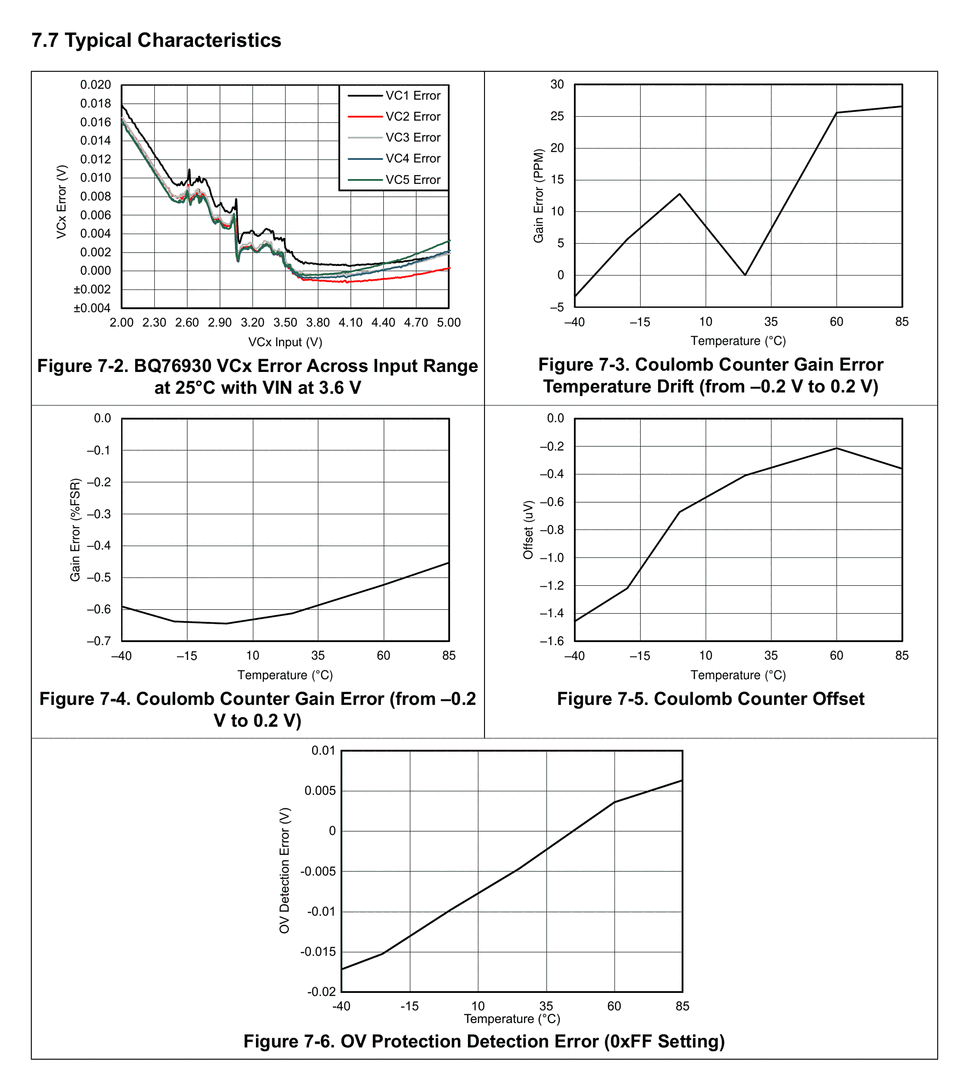
| ADC accuracy at 25 °C | V_CELL = 2.0 V to 5.0 V | — | ±25 | — | mV |
| ADC accuracy 0 °C to 60 °C | V_CELL = 2.0 V to 5.0 V | — | ±25 | — | mV |
| ADC accuracy −40 °C to 85 °C | V_CELL = 2.0 V to 5.0 V | −50 | ±35 | 50 | mV |
Coulomb-counter current measurement
| Parameter | Test Condition | Min | Typ | Max | Unit |
|---|---|---|---|---|---|
| CC input range | −200 | — | 200 | mV | |
| CC full scale | −270 | — | 270 | mV | |
| CC LSB | — | 8.44 | — | µV | |
| CC conversion time | Single conversion | — | 250 | — | ms |
| Integral non-linearity | 16-bit fit over input voltage range ±200 mV | — | ±2 | ±40 | LSB |
| Offset error | — | ±1 | ±3 | LSB | |
| Gain error | Over input voltage range | −0.5 | — | +0.5 | % FSR |
| Gain error drift | — | — | ±150 | PPM/°C | |
| Effective input resistance | 2.5 | — | — | MΩ |
Voltage protections (OV / UV / OCD / SCD)
| Parameter | Test Condition | Min | Typ | Max | Unit |
|---|---|---|---|---|---|
| OV_RANGE | OV threshold range | 0x2008 | — | 0x2FFE | ADC |
| UV_RANGE | UV threshold range | 0x1000 | — | 0x1FF0 | ADC |
| OV_SYSTEP | OV and UV threshold step size | — | 16 | — | LSB |
| UV_MNDUAL | UV minimum value to qualify | — | 0x0518 | — | ADC |
| OV_DELAY | OV delay time options | 1 s / 2 s / 4 s / 8 s | |||
| UV_DELAY | UV delay time options | 1 s / 4 s / 8 s / 16 s | |||
| OCD_RANGE | OCD threshold range | 8 | — | 100 | mV |
| OCD_STEP | OCD threshold step size | — | 2.78 / 5.56 | — | mV |
| OCD_DELAY | Delay options | 8 / 22 / 200 / 1280 | ms | ||
| SCD_RANGE | SCD threshold range | 22 | — | 200 | mV |
| SCD_STEP | Step size | 11.1 / 22.2 | mV | ||
| SCD_DELAY | Delay options | 35 / 50 / 70 / 100 / 140 / 200 / 280 / 400 | µs |
Thermal Information
| Thermal Metric | BQ76920 (20-TSSOP PW) | BQ76930 (30-TSSOP DBT) | BQ76940 (44-TSSOP DBT) | Unit |
|---|---|---|---|---|
| R_θJA Junction-to-ambient thermal resistance | 93.7 | 86.5 | 79.1 | °C/W |
| R_θJC(top) Junction-to-case (top) | 28.7 | 19.4 | 17.5 | °C/W |
| R_θJB Junction-to-board | 44.6 | 41.3 | 33.9 | °C/W |
| ψ_JT Junction-to-top characterization | 1.3 | 0.5 | 0.5 | °C/W |
| ψ_JB Junction-to-board characterization | 44.1 | 40.6 | 33.4 | °C/W |
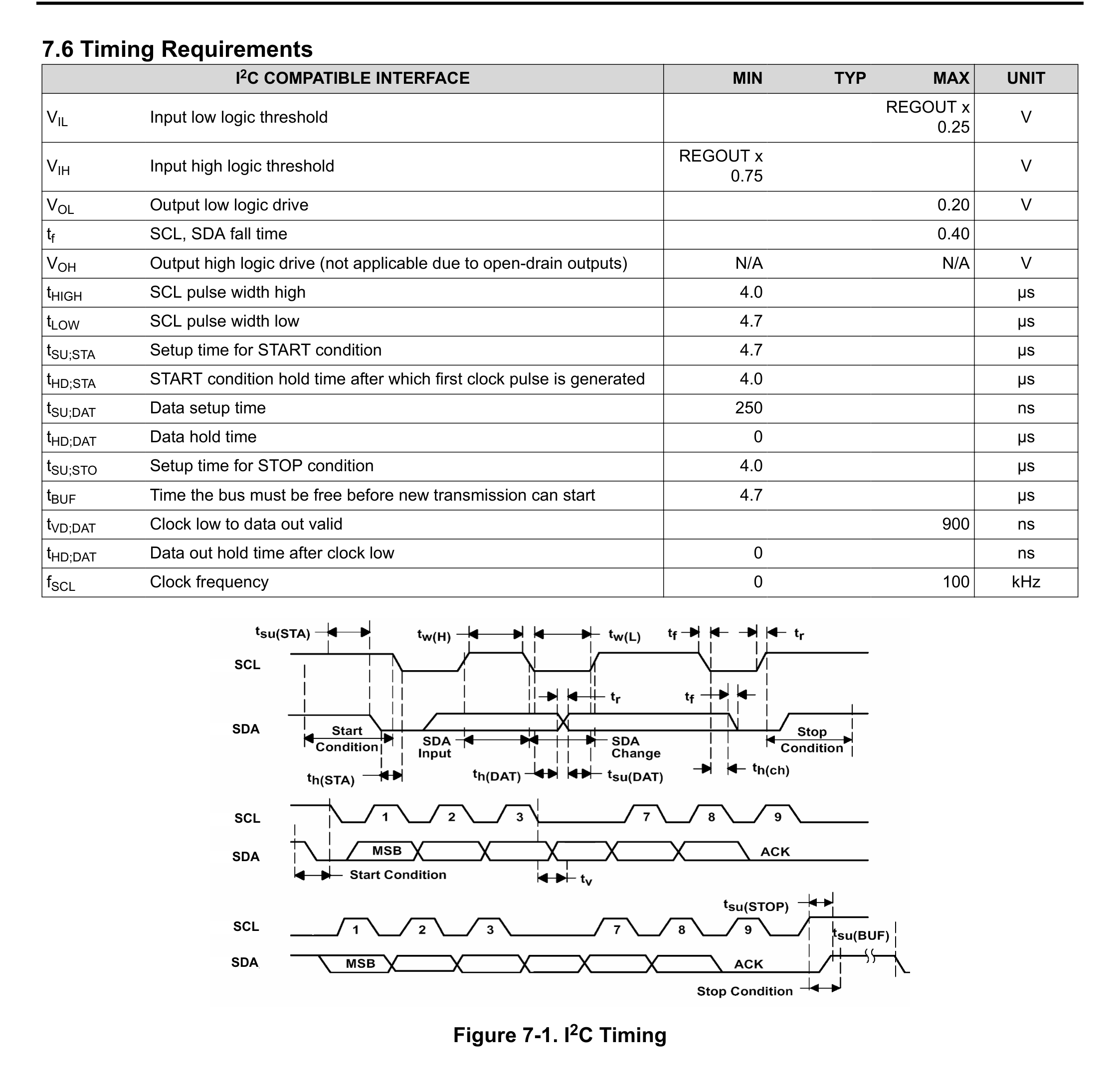
Timing Requirements
I²C-compatible interface. Typical conditions: T_A = 25 °C.
| Parameter | Min | Typ | Max | Unit |
|---|---|---|---|---|
| V_IL Input low logic threshold | — | — | REGOUT × 0.25 | V |
| V_IH Input high logic threshold | REGOUT × 0.75 | — | — | V |
| V_OL Output low logic drive | — | — | 0.20 | V |
| t_r SCL, SDA fall time | — | — | 0.40 | µs |
| V_OH Output high logic drive (not applicable due to open-drain) | N/A | N/A | N/A | V |
| t_HIGH SCL pulse width high | 4.0 | — | — | µs |
| t_LOW SCL pulse width low | 4.7 | — | — | µs |
| t_SU,STA Setup time for START condition | 4.7 | — | — | µs |
| t_HD,STA START condition hold time after first clock pulse is generated | 4.0 | — | — | µs |
| t_SU,DAT Data setup time | 250 | — | — | ns |
| t_HD,DAT Data hold time | 0 | — | — | µs |
| t_SU,STO Setup time for STOP condition | 4.0 | — | — | µs |
| t_BUF Bus free time between new transmission can start | 4.7 | — | — | µs |
| t_HD,DAT Data out hold time after clock low | 0 | — | — | µs |
| t_VD,DAT Data out valid time after clock low | — | — | 900 | ns |
| f_SCL Clock frequency | 0 | — | 100 | kHz |
Packages
| Part Number (T&R) | Family Variant | Cells | I²C Addr | LDO | CRC | Package |
|---|---|---|---|---|---|---|
| BQ7692000PWR | BQ76920 | 3–5 | 0x08 | 2.5 V | No | 20-TSSOP (PW) |
| BQ7692001PWR | BQ76920 | 3–5 | 0x08 | 2.5 V | Yes | 20-TSSOP (PW) |
| BQ7692002PWR | BQ76920 | 3–5 | 0x08 | 3.3 V | No | 20-TSSOP (PW) |
| BQ7692003PWR | BQ76920 | 3–5 | 0x08 | 3.3 V | Yes | 20-TSSOP (PW) |
| BQ7692006PWR | BQ76920 | 3–5 | 0x18 | 3.3 V | No | 20-TSSOP (PW) |
| BQ7693000DBTR | BQ76930 | 6–10 | 0x08 | 2.5 V | No | 30-TSSOP (DBT) |
| BQ7693003DBTR | BQ76930 | 6–10 | 0x08 | 3.3 V | Yes | 30-TSSOP (DBT) |
| BQ7694000DBTR | BQ76940 | 9–15 | 0x08 | 2.5 V | No | 44-TSSOP (DBT) |
| BQ7694003DBTR | BQ76940 | 9–15 | 0x08 | 3.3 V | Yes | 44-TSSOP (DBT) |
Package dimensions:
| Package | Pins | Body Size |
|---|---|---|
| TSSOP (PW) | 20 | 6.50 mm × 4.40 mm × 1.20 mm |
| TSSOP (DBT) | 30 | 7.80 mm × 4.40 mm × 1.20 mm |
| TSSOP (DBT) | 44 | 11.00 mm × 4.40 mm × 1.20 mm |
Applications
- Light electric vehicles (LEV): eBikes, eScooters, pedelecs, pedal-assist bicycles
- Power tools and garden tools
- Battery backup units (BBU), energy storage systems (ESS), uninterruptible power supply (UPS) systems
- Industrial battery packs (3-cell and up; use BQ76930/BQ76940 for ≥6-cell packs)
Communication Interface
The BQ7692003PWR variant communicates via I²C at the fixed 7-bit address 0x08, with CRC enabled on every register read and write. The slave address is factory-set — this variant cannot be changed to 0x18 at runtime; use the BQ7692006PWR variant if a 0x18 address is required.
Register map spans 0x00–0x3B, covering:
- System status (SYS_STAT) and ALERT mask (SYS_CTRL1/2)
- OV / UV / SCD / OCD protection thresholds and delay settings
- Cell voltages VC1..VC5 (14-bit, 382 µV LSB)
- Coulomb-counter current (16-bit, 8.44 µV LSB) — paired with sense resistor R_SNS
- Temperature sensor channels
- Cell balancing enable per cell (CELLBAL1)
- I²C CRC control
Key Formulas
Cell voltage ADC conversion
$$V_{CELL} = ADC_{GAIN} \times ADC_{CODE} + ADC_{OFFSET}$$
where ADC_GAIN ≈ 382 µV/LSB and ADC_OFFSET is read from ADCOFFSET register (signed mV).
Coulomb-counter current
$$I_{PACK} = \frac{CC_{CODE} \times 8.44\ \mu V}{R_{SNS}}$$
where R_SNS is the external sense resistor (typically 1–10 mΩ).
OCD and SCD thresholds
$$V_{OCD} = OCD_{RANGE_{LSB}} \times OCD_{STEP}$$
$$V_{SCD} = SCD_{RANGE_{LSB}} \times SCD_{STEP}$$
Trip current is then V_threshold / R_SNS.
Troubleshooting
| Symptom | Cause | Fix |
|---|---|---|
| Device does not respond on I²C | Incorrect address or CRC setting for the variant | BQ7692003PWR uses address 0x08 with CRC enabled — all reads/writes must include CRC byte |
| ADC readings drift with temperature | Thermistor TS1 floating or filter caps wrong | Pull TS1 to VSS through 10 kΩ if unused; verify C_C per recommended operating conditions |
| FET drivers not engaging | CHG/DSG disabled via SYS_CTRL2 or protection fault latched | Read SYS_STAT; clear latched protection bits by writing 1 to the corresponding SYS_STAT bit |
| Coulomb counter reads 0 | CC not enabled | Set CC_EN in SYS_CTRL2; allow one 250 ms conversion cycle |
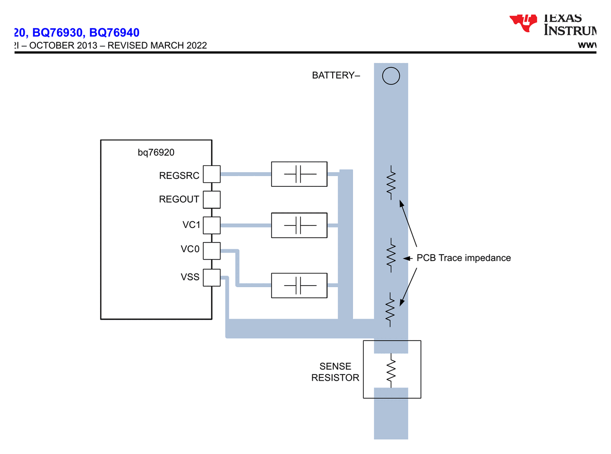
| Large pack parasitic impedance causes voltage errors | Input cap grounding runs across sense resistor | Route cell input caps to local ground between battery tab and sense resistor (see layout example in datasheet §11) |