XBLW ULN2003AB
Seven-channel Darlington transistor array — 500mA/ch, 50V, TTL/CMOS input, integrated clamp diodes, DIP-16/SOP-16
Paste this into Claude Code (VS Code panel, Adom editor, or terminal) to install:
Search the Adom Wiki for the datasheet "XBLW ULN2003AB" (slug: uln2003ab) at https://wiki-ufypy5dpx93o.adom.cloud/wiki/datasheets/uln2003ab. Download the standardized markdown and extracted diagram images into my project's datasheets/uln2003ab/ directory. Show me the key specifications and pin configuration.
Description
The XBLW ULN2003AB is a seven-channel high-voltage, high-current Darlington transistor array from Xinbole (XBLW). Each channel features an open-collector Darlington pair with common emitters, rated at 500 mA continuous output current (600 mA peak). Integrated suppression (free-wheeling) diodes on each output provide protection for inductive load driving. Input pins are compatible with TTL and CMOS logic levels. Available in DIP-16 and SOP-16 packages.
Features
- • Seven Darlington transistor channels with open-collector outputs
- • Output current: 500 mA per channel (continuous)
- • Collector-emitter voltage withstand: 50 V
- • Input compatible with TTL/CMOS logic signals (5V)
- • Integrated clamp diodes for inductive load suppression
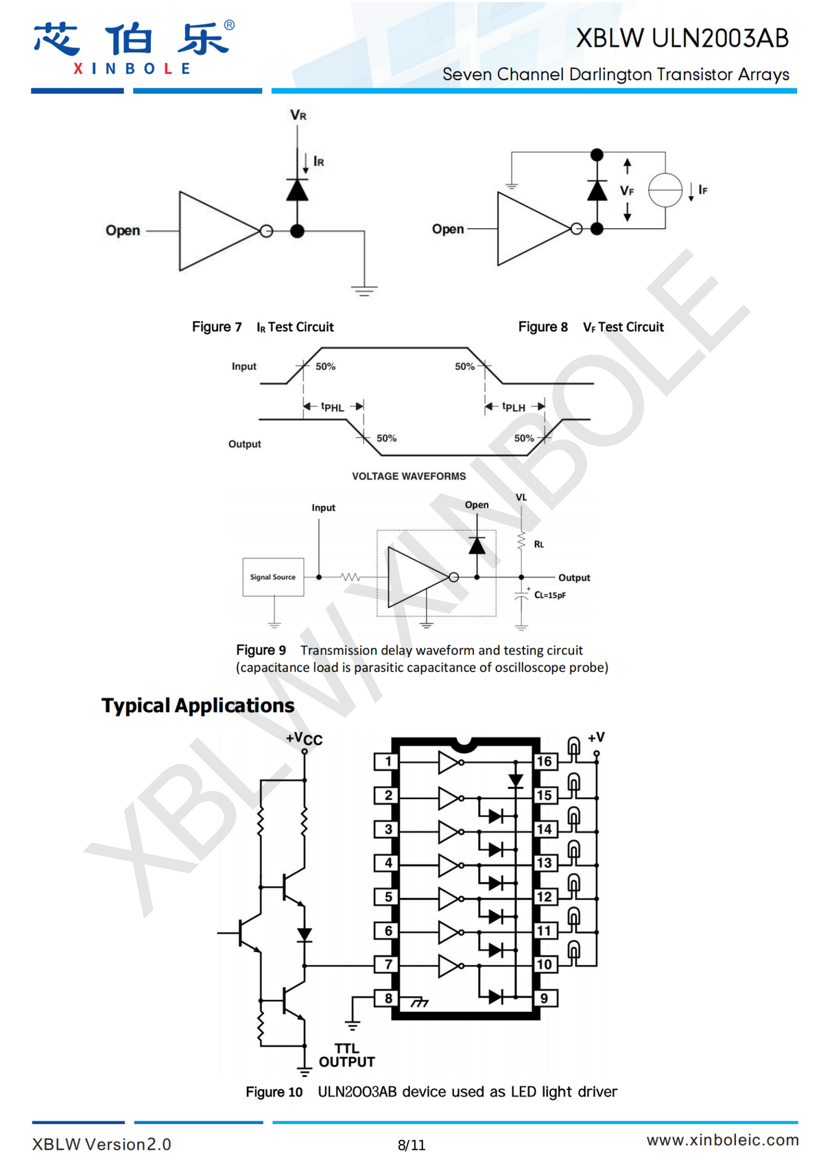
- • Propagation delay: 0.15 us typical (tPLH/tPHL)
- • Available in DIP-16 and SOP-16 packages
- • RoHS compliant
Pin Configuration
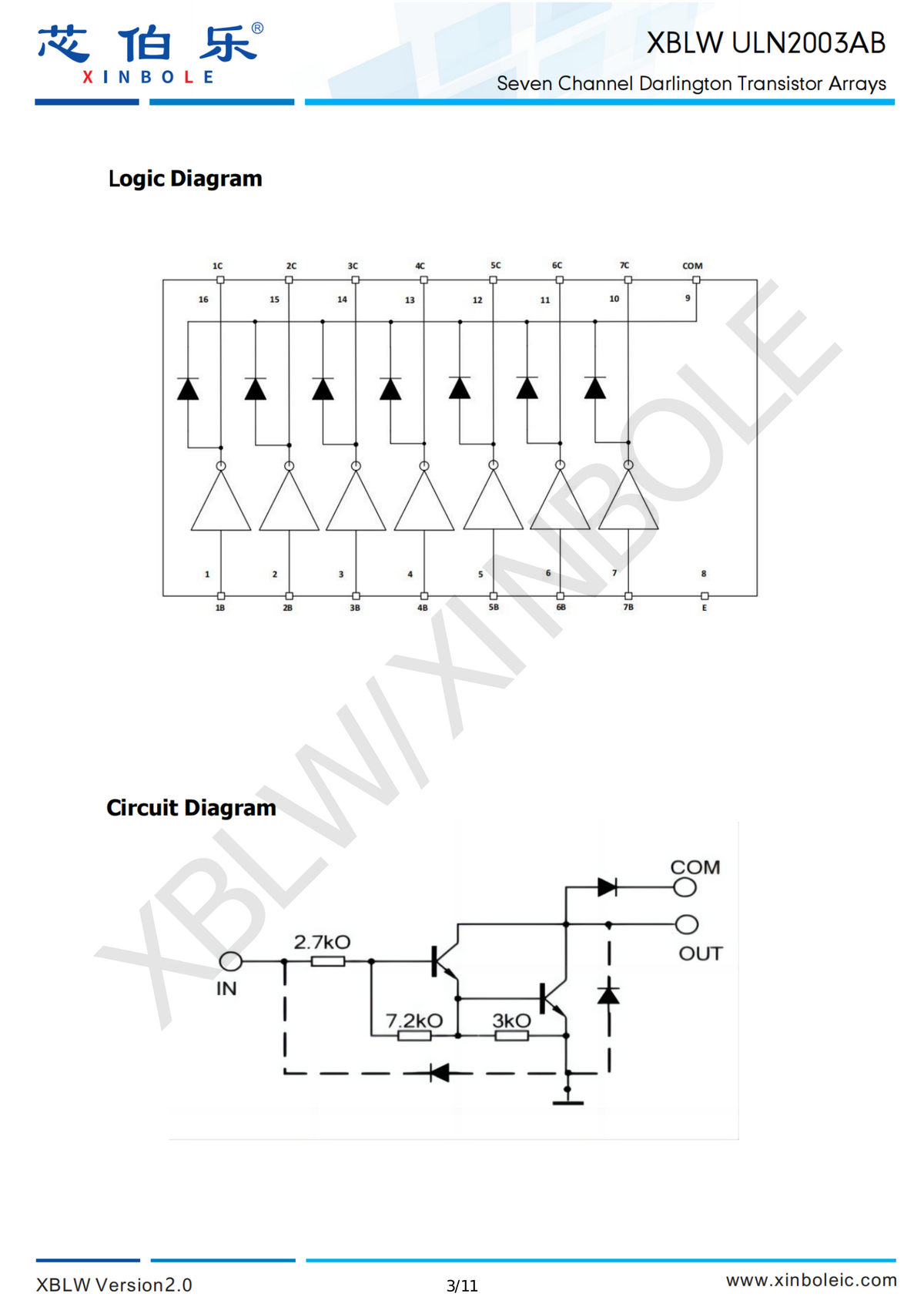
Each channel includes a 2.7 kOhm input resistor, 7.2 kOhm base-emitter resistor, and 3 kOhm feedback resistor in the Darlington configuration.
Absolute Maximum Ratings
Ta = 25 C
| Parameter | Symbol | Value | Unit |
|---|---|---|---|
| Collector-emitter voltage | VCE | 50 | V |
| COM voltage | VCOM | 50 | V |
| Input voltage | VI | 30 | V |
| Collector peak current | ICP | 500 | mA |
| Output clamp current | IOK | 500 | mA |
| Emitter maximum current | IET | -2.5 | A |
| Junction-to-ambient thermal resistance (SOP-16) | theta_JA | 63 | C/W |
| Junction-to-ambient thermal resistance (DIP-16) | theta_JA | 50 | C/W |
| Maximum junction temperature | TJ | 150 | C |
| Welding temperature (10s) | TW | 260 | C |
| Storage temperature range | TS | -65 to +150 | C |
Recommended Operating Conditions
Ta = 25 C unless otherwise noted.
| Parameter | Symbol | Min | Max | Unit | Conditions |
|---|---|---|---|---|---|
| Collector-emitter voltage | VCE | 0 | 50 | V | |
| Output current | IOUT | -- | 100 | mA/ch | TA = +85 C, TJ = 120 C |
| Input voltage | VIN | 0 | 24 | V | |
| Input voltage (output on) | VIN(ON) | 2.8 | 24 | V | IOUT = 400 mA |
| Input voltage (output off) | VIN(OFF) | 0 | 0.7 | V | |
| Clamp diode reverse voltage | VR | -- | 50 | V | |
| Clamp forward current | IF | -- | 350 | mA | |
| Operating temperature range | TA | -20 | +85 | C | |
| Storage temperature range | TJ | -20 | +125 | C | |
| Power dissipation (SOP-16) | PD | -- | 1.25 | W | TA = +25 C |
| Power dissipation (SOP-16) | PD | -- | 0.65 | W | TA = +85 C |
| Power dissipation (DIP-16) | PD | -- | 1.47 | W | TA = +25 C |
| Power dissipation (DIP-16) | PD | -- | 0.76 | W | TA = +85 C |
Electrical Characteristics
Ta = 25 C
| Parameter | Symbol | Test Conditions | Typ | Max | Unit |
|---|---|---|---|---|---|
| On-state input voltage | VIN(ON) | VCE = 2V, IC = 200 mA | 1.9 | 2.4 | V |
| On-state input voltage | VIN(ON) | VCE = 2V, IC = 250 mA | 2 | 2.7 | V |
| On-state input voltage | VIN(ON) | VCE = 2V, IC = 300 mA | 2.1 | 3 | V |
| CE saturation voltage | VCE(SAT) | VI = 2.4V, IC = 30 mA | 0.78 | 1 | V |
| CE saturation voltage | VCE(SAT) | VI = 2.4V, IC = 60 mA | 0.82 | 1.1 | V |
| CE saturation voltage | VCE(SAT) | VI = 2.4V, IC = 120 mA | 0.9 | 1.2 | V |
| CE saturation voltage | VCE(SAT) | VI = 2.4V, IC = 240 mA | 1.1 | 1.4 | V |
| CE saturation voltage | VCE(SAT) | VI = 2.4V, IC = 350 mA | 1.25 | 1.6 | V |
| Input current | II | IC = 60 mA, VI = 12V | 4 | 5.3 | mA |
| Input current | II | IC = 60 mA, VI = 6V | 1.7 | 2.2 | mA |
| Input current | II | IC = 60 mA, VI = 4.5V | 1.1 | 1.6 | mA |
| Input current | II | IC = 60 mA, VI = 2.4V | 0.35 | 0.7 | mA |
| Clamp forward voltage | VF | IF = 350 mA | 1.6 | 2 | V |
| Collector cutoff current | ICEX | VCE = 50V, II = 0 | -- | 50 | uA |
| Clamp reverse current | IR | VR = 50V | -- | 50 | uA |
| Propagation delay (low-to-high) | tPLH | VL = 12V, RL = 45 ohm | 0.15 | 1 | us |
| Propagation delay (high-to-low) | tPHL | VL = 12V, RL = 45 ohm | 0.15 | 1 | us |
Packages
Ordering Information
| Product Model | Package | Marking | Packing | Qty |
|---|---|---|---|---|
| XBLW ULN2003ABN | DIP-16 | ULN2003ABN | Tube | 1000 pcs/box |
| XBLW ULN2003ABDTR | SOP-16 | ULN2003AB | Tape | 2500 pcs/reel |
DIP-16 Dimensions
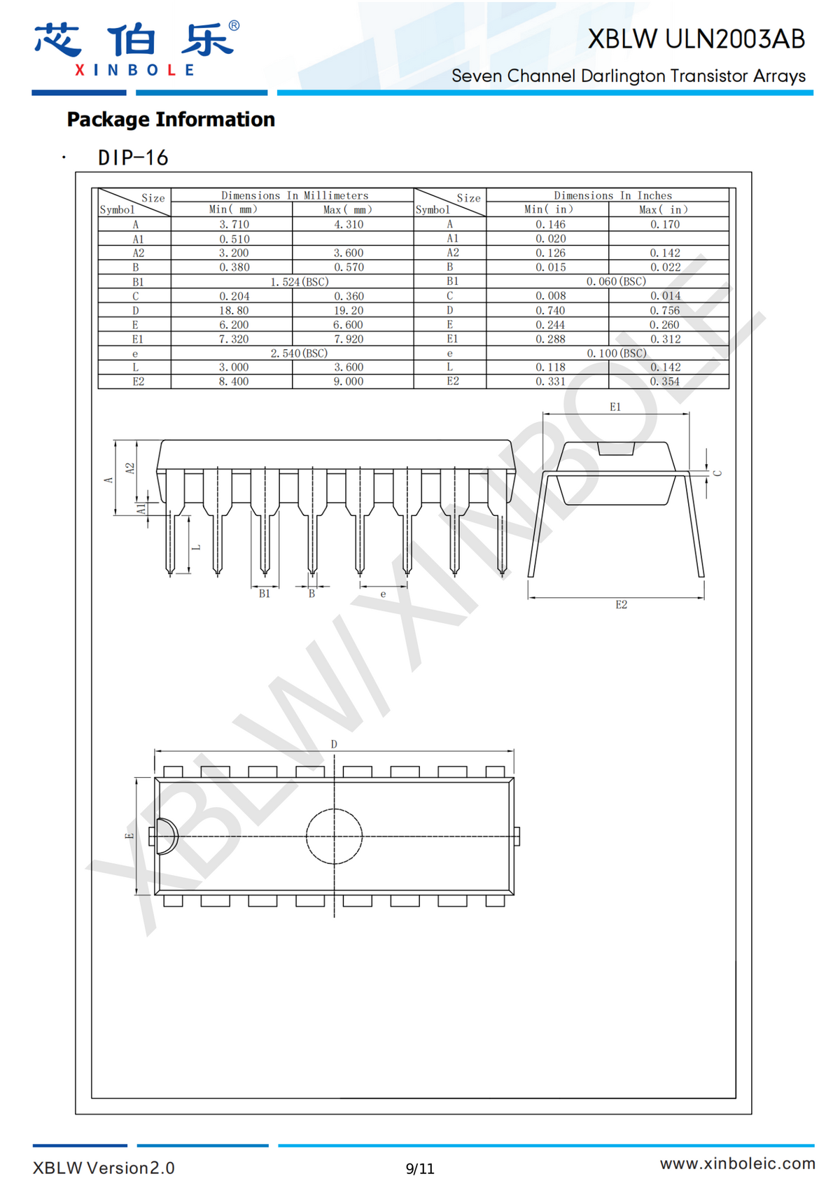
Body: 18.80-19.20 mm (D) x 6.20-6.60 mm (E). Height: 3.71-4.31 mm (A). Lead pitch: 2.54 mm (BSC). Lead width: 0.38-0.57 mm (B).
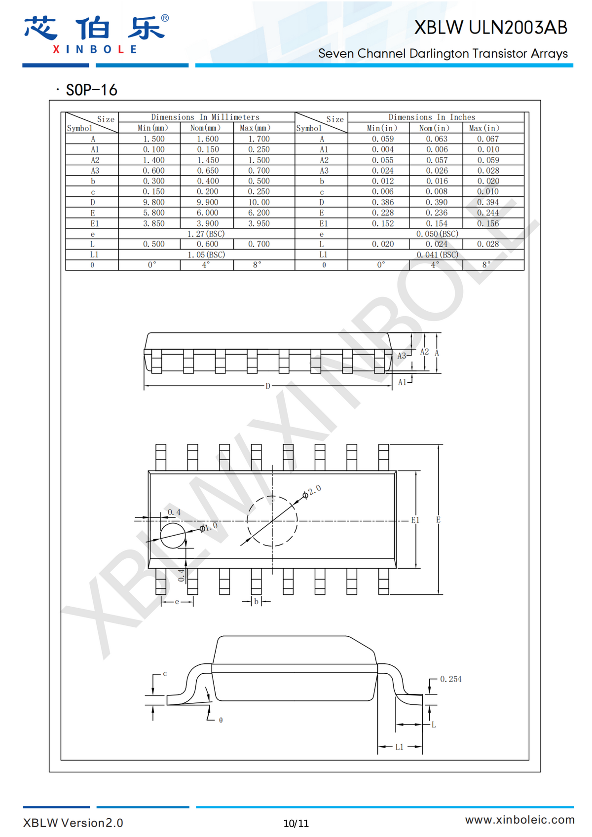
SOP-16 Dimensions
Body: 9.80-10.00 mm (D) x 5.80-6.20 mm (E). Height: 1.50-1.70 mm (A). Lead pitch: 1.27 mm (BSC). Lead width: 0.30-0.50 mm (b).
Applications
- Relay drivers
- Lamp and LED drivers
- Display drivers
- Stepper motor drivers
- Logic level shifting (TTL/CMOS to high-voltage loads)
- General-purpose high-side inductive load switching
Diagrams & Graphs (5)
## Description

The XBLW ULN2003AB is a seven-channel high-voltage, high-current Darlington transistor array from Xinbole (XBLW). Each channel features an open-collector Darlington pair with common emitters, rated at 500 mA continuous output current (600 mA peak). Integrated suppression (free-wheeling) diodes on each output provide protection for inductive load driving. Input pins are compatible with TTL and CMOS logic levels. Available in DIP-16 and SOP-16 packages.

## Features

- Seven Darlington transistor channels with open-collector outputs
- Output current: 500 mA per channel (continuous)
- Collector-emitter voltage withstand: 50 V
- Input compatible with TTL/CMOS logic signals (5V)
- Integrated clamp diodes for inductive load suppression
- Propagation delay: 0.15 us typical (tPLH/tPHL)
- Available in DIP-16 and SOP-16 packages
- RoHS compliant

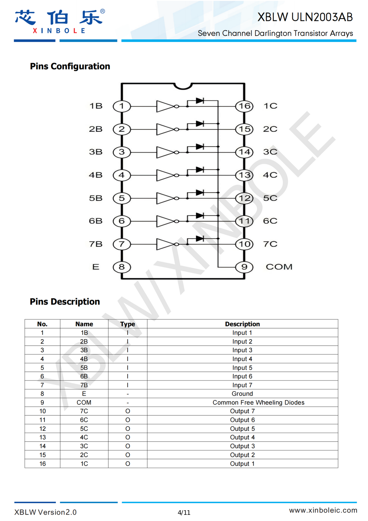
## Pin Configuration

| Pin | Name | Type | Description |
|-----|------|------|-------------|
| 1 | 1B | I | Input 1 |
| 2 | 2B | I | Input 2 |
| 3 | 3B | I | Input 3 |
| 4 | 4B | I | Input 4 |
| 5 | 5B | I | Input 5 |
| 6 | 6B | I | Input 6 |
| 7 | 7B | I | Input 7 |
| 8 | E | - | Ground (common emitter) |
| 9 | COM | - | Common free-wheeling diodes |
| 10 | 7C | O | Output 7 |
| 11 | 6C | O | Output 6 |
| 12 | 5C | O | Output 5 |
| 13 | 4C | O | Output 4 |
| 14 | 3C | O | Output 3 |
| 15 | 2C | O | Output 2 |
| 16 | 1C | O | Output 1 |

Each channel includes a 2.7 kOhm input resistor, 7.2 kOhm base-emitter resistor, and 3 kOhm feedback resistor in the Darlington configuration.

## Absolute Maximum Ratings

Ta = 25 C

| Parameter | Symbol | Value | Unit |
|-----------|--------|-------|------|
| Collector-emitter voltage | VCE | 50 | V |
| COM voltage | VCOM | 50 | V |
| Input voltage | VI | 30 | V |
| Collector peak current | ICP | 500 | mA |
| Output clamp current | IOK | 500 | mA |
| Emitter maximum current | IET | -2.5 | A |
| Junction-to-ambient thermal resistance (SOP-16) | theta_JA | 63 | C/W |
| Junction-to-ambient thermal resistance (DIP-16) | theta_JA | 50 | C/W |
| Maximum junction temperature | TJ | 150 | C |
| Welding temperature (10s) | TW | 260 | C |
| Storage temperature range | TS | -65 to +150 | C |

## Recommended Operating Conditions

Ta = 25 C unless otherwise noted.

| Parameter | Symbol | Min | Max | Unit | Conditions |
|-----------|--------|-----|-----|------|------------|
| Collector-emitter voltage | VCE | 0 | 50 | V | |
| Output current | IOUT | -- | 100 | mA/ch | TA = +85 C, TJ = 120 C |
| Input voltage | VIN | 0 | 24 | V | |
| Input voltage (output on) | VIN(ON) | 2.8 | 24 | V | IOUT = 400 mA |
| Input voltage (output off) | VIN(OFF) | 0 | 0.7 | V | |
| Clamp diode reverse voltage | VR | -- | 50 | V | |
| Clamp forward current | IF | -- | 350 | mA | |
| Operating temperature range | TA | -20 | +85 | C | |
| Storage temperature range | TJ | -20 | +125 | C | |
| Power dissipation (SOP-16) | PD | -- | 1.25 | W | TA = +25 C |
| Power dissipation (SOP-16) | PD | -- | 0.65 | W | TA = +85 C |
| Power dissipation (DIP-16) | PD | -- | 1.47 | W | TA = +25 C |
| Power dissipation (DIP-16) | PD | -- | 0.76 | W | TA = +85 C |

## Electrical Characteristics

Ta = 25 C

| Parameter | Symbol | Test Conditions | Typ | Max | Unit |
|-----------|--------|----------------|-----|-----|------|
| On-state input voltage | VIN(ON) | VCE = 2V, IC = 200 mA | 1.9 | 2.4 | V |
| On-state input voltage | VIN(ON) | VCE = 2V, IC = 250 mA | 2 | 2.7 | V |
| On-state input voltage | VIN(ON) | VCE = 2V, IC = 300 mA | 2.1 | 3 | V |
| CE saturation voltage | VCE(SAT) | VI = 2.4V, IC = 30 mA | 0.78 | 1 | V |
| CE saturation voltage | VCE(SAT) | VI = 2.4V, IC = 60 mA | 0.82 | 1.1 | V |
| CE saturation voltage | VCE(SAT) | VI = 2.4V, IC = 120 mA | 0.9 | 1.2 | V |
| CE saturation voltage | VCE(SAT) | VI = 2.4V, IC = 240 mA | 1.1 | 1.4 | V |
| CE saturation voltage | VCE(SAT) | VI = 2.4V, IC = 350 mA | 1.25 | 1.6 | V |
| Input current | II | IC = 60 mA, VI = 12V | 4 | 5.3 | mA |
| Input current | II | IC = 60 mA, VI = 6V | 1.7 | 2.2 | mA |
| Input current | II | IC = 60 mA, VI = 4.5V | 1.1 | 1.6 | mA |
| Input current | II | IC = 60 mA, VI = 2.4V | 0.35 | 0.7 | mA |
| Clamp forward voltage | VF | IF = 350 mA | 1.6 | 2 | V |
| Collector cutoff current | ICEX | VCE = 50V, II = 0 | -- | 50 | uA |
| Clamp reverse current | IR | VR = 50V | -- | 50 | uA |
| Propagation delay (low-to-high) | tPLH | VL = 12V, RL = 45 ohm | 0.15 | 1 | us |
| Propagation delay (high-to-low) | tPHL | VL = 12V, RL = 45 ohm | 0.15 | 1 | us |

## Packages

### Ordering Information

| Product Model | Package | Marking | Packing | Qty |
|--------------|---------|---------|---------|-----|
| XBLW ULN2003ABN | DIP-16 | ULN2003ABN | Tube | 1000 pcs/box |
| XBLW ULN2003ABDTR | SOP-16 | ULN2003AB | Tape | 2500 pcs/reel |

### DIP-16 Dimensions

Body: 18.80-19.20 mm (D) x 6.20-6.60 mm (E). Height: 3.71-4.31 mm (A). Lead pitch: 2.54 mm (BSC). Lead width: 0.38-0.57 mm (B).

### SOP-16 Dimensions

Body: 9.80-10.00 mm (D) x 5.80-6.20 mm (E). Height: 1.50-1.70 mm (A). Lead pitch: 1.27 mm (BSC). Lead width: 0.30-0.50 mm (b).

## Applications

- Relay drivers
- Lamp and LED drivers
- Display drivers
- Stepper motor drivers
- Logic level shifting (TTL/CMOS to high-voltage loads)
- General-purpose high-side inductive load switching
Sub-Skills
What are Sub-Skills?
Sub-skills are community-contributed AI skill extensions for this component.
They teach AI assistants about specific tools, configurators, or workflows.
Examples:
- A manufacturer’s configuration tool for a motor controller
- A community-written design guide for an amplifier circuit
- An automated test/validation script for a sensor module
How to add one: Click Add Sub-Skill, provide the URL
to your skill and a brief description. Submissions are reviewed by the Adom team
before going live.
Sub-skills are community-contributed AI skill extensions for this component. They teach AI assistants about specific tools, configurators, or workflows.
Examples:
- A manufacturer’s configuration tool for a motor controller
- A community-written design guide for an amplifier circuit
- An automated test/validation script for a sensor module
How to add one: Click Add Sub-Skill, provide the URL to your skill and a brief description. Submissions are reviewed by the Adom team before going live.
No sub-skills yet. Be the first to contribute one!