SiR680ADP
N-Channel 80V MOSFET — 2.35mOhm RDS(on), 100A, PowerPAK SO-8, TrenchFET Gen IV, sync rect/DC-DC
Paste this into Claude Code (VS Code panel, Adom editor, or terminal) to install:
Search the Adom Wiki for the datasheet "SiR680ADP" (slug: sir680adp) at https://wiki-ufypy5dpx93o.adom.cloud/wiki/datasheets/sir680adp. Download the standardized markdown and extracted diagram images into my project's datasheets/sir680adp/ directory. Show me the key specifications and pin configuration.
Description
The SiR680ADP is a high-performance N-channel 80 V power MOSFET from Vishay Siliconix in a PowerPAK SO-8 single package. Built on Vishay's TrenchFET Gen IV technology, it is optimized for the lowest RDS(on) x Qg and RDS(on) x Qoss figures of merit (FOM), making it ideal for synchronous rectification, primary-side switching, and DC-DC converter applications. The device delivers extremely low on-resistance (2.35 mOhm typical at VGS = 10 V) with a continuous drain current rating of 100 A at 25 C.
Features
- • TrenchFET Gen IV power MOSFET technology
- • Very low RDS(on): 2.35 mOhm typ at VGS = 10 V, ID = 20 A
- • Low RDS(on) x Qg figure of merit
- • Tuned for lowest RDS(on) x Qoss FOM
- • 100% Rg and UIS tested
- • Continuous drain current: 100 A (at 25 C case temperature)
- • Drain-source voltage: 80 V
- • Gate-source voltage: +/- 20 V
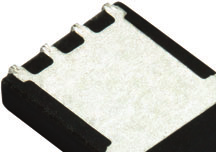
- • PowerPAK SO-8 package (leadless, exposed copper pad)
- • RoHS compliant, halogen-free
Pin Configuration
PowerPAK SO-8 Single configuration:
| Pin | Function |
|---|---|
| 1 | S (Source) |
| 2 | S (Source) |
| 3 | S (Source) |
| 4 | G (Gate) |
| 5 | D (Drain) |
| 6 | D (Drain) |
| 7 | D (Drain) |
| 8 | D (Drain) |
| Exposed pad | D (Drain) |
Absolute Maximum Ratings
TA = 25 C unless otherwise noted.
| Parameter | Symbol | Limit | Unit |
|---|---|---|---|
| Drain-source voltage | VDS | 80 | V |
| Gate-source voltage | VGS | +/- 20 | V |
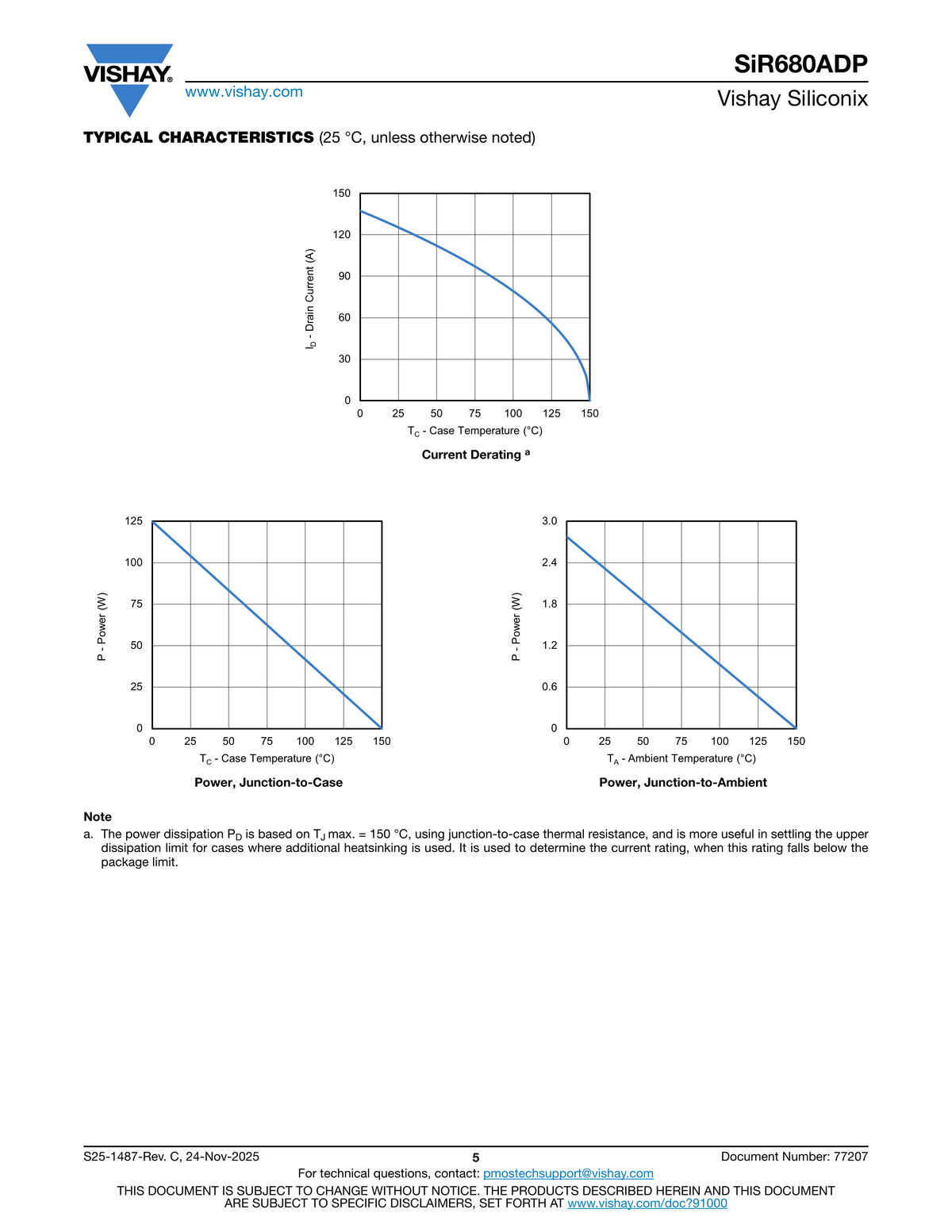
| Continuous drain current (TC = 25 C) | ID | 100 | A |
| Continuous drain current (TC = 70 C) | ID | 80.7 | A |
| Continuous drain current (TA = 25 C) | ID | 24.5 | A |
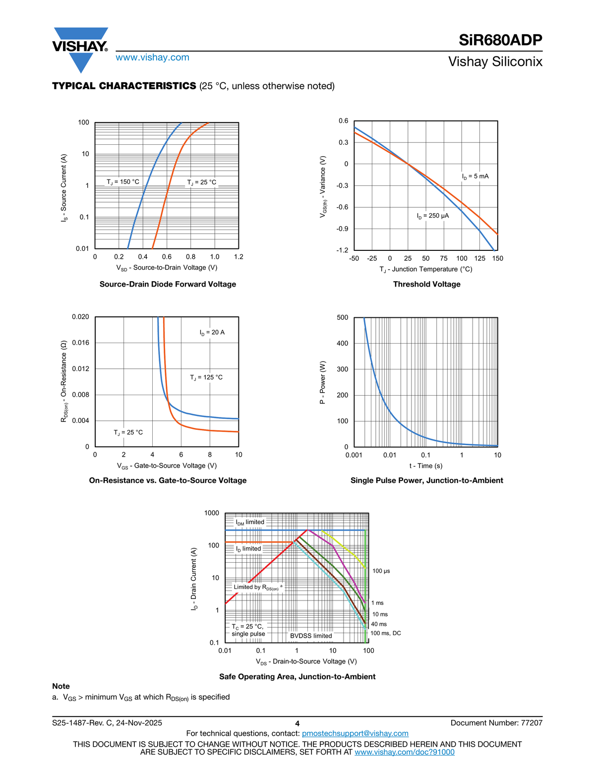
| Pulsed drain current (t <= 100 us) | IDM | 300 | A |
| Continuous source-drain diode current | IS | 5.6 | A |
| Single pulse avalanche current (L = 0.1 mH) | IAS | 80 | mJ |
| Single pulse avalanche energy | EAS | 104 | mJ |
| Maximum power dissipation (TC = 25 C) | PD | 125 | W |
| Maximum power dissipation (TC = 70 C) | PD | 68.6 | W |
| Maximum power dissipation (TA = 25 C) | PD | 6.25 | W |
| Maximum power dissipation (TA = 70 C) | PD | 4.1 | W |
| Operating junction and storage temperature | TJ, Tstg | -55 to +150 | C |
| Soldering recommendations (peak temperature) | - | 260 | C |
Thermal Information
| Parameter | Symbol | Typical | Maximum | Unit |
|---|---|---|---|---|
| Maximum junction-to-ambient (t <= 10 s) | RthJA | - | 20 | C/W |
| Maximum junction-to-case (drain) steady state | RthJC | 0.9 | 1.2 | C/W |
Electrical Characteristics
TJ = 25 C unless otherwise noted.
Static
| Parameter | Symbol | Test Conditions | Min | Typ | Max | Unit |
|---|---|---|---|---|---|---|
| Drain-source breakdown voltage | V(BR)DSS | VGS = 0 V, ID = 1 mA | 80 | -- | -- | V |
| VDS temperature coefficient | dV(BR)/dT | ID = 10 mA | -- | 61 | -- | mV/C |
| V(BR)DSS temperature coefficient | dV(BR)DSS/TJ | ID = 250 uA | -- | -8.2 | -- | mV/C |
| Gate-source threshold voltage | VGS(th) | VDS = VGS, ID = 250 uA | 2 | -- | 3.5 | V |
| Gate-source leakage | IGSS | VGS = +/- 20 V | -- | -- | 100 | nA |
| Zero gate voltage drain current | IDSS | VGS = 0 V | -- | -- | 1 | uA |
| On-state drain current | ID(on) | VGS = 10 V, VDS = 0.1 V | -- | 40 | -- | A |
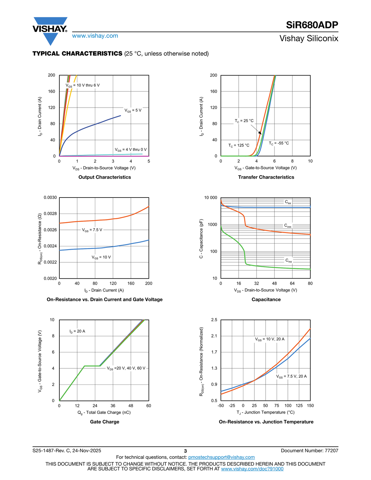
| Drain-source on-resistance | RDS(on) | VGS = 10 V, ID = 20 A | -- | 0.00235 | 0.00288 | Ohm |
| Drain-source on-resistance | RDS(on) | VGS = 7.5 V, ID = 15 A | -- | 0.00270 | 0.00350 | Ohm |
| Forward transconductance | gfs | VDS = 15 V, ID = 20 A | -- | 68 | -- | S |
Dynamic
| Parameter | Symbol | Test Conditions | Min | Typ | Max | Unit |
|---|---|---|---|---|---|---|
| Input capacitance | Ciss | VGS = 0 V, f = 1 MHz | -- | 4415 | -- | pF |
| Output capacitance | Coss | VDS = 40 V | -- | 614 | -- | pF |
| Reverse transfer capacitance | Crss | -- | 26 | -- | pF | |
| Total gate charge | Qg | VDS = 40 V, ID = 20 A | -- | 55 | 83 | nC |
| Gate-source charge | Qgs | VGS = 10 V | -- | 43 | 65 | nC |
| Gate-drain charge | Qgd | -- | 17 | -- | nC | |
| Gate resistance | Rg | f = 1 MHz | 0.3 | 0.88 | 1.5 | Ohm |
| Turn-on delay time | td(on) | VDD = 40 V, RL = 2 Ohm | -- | 17 | 34 | ns |
| Rise time | tr | ID = 20 A, RG = 1 Ohm | -- | 8 | 16 | ns |
| Turn-off delay time | td(off) | -- | 30 | 60 | ns | |
| Fall time | tf | -- | 9 | 18 | ns | |
| Turn-on delay time | td(on) | VDD = 40 V, RL = 2 Ohm | -- | 15 | 30 | ns |
| Rise time | tr | RG = 7.5 V, RG = 1 Ohm | -- | 9 | 18 | ns |
| Turn-off delay time | td(off) | -- | 30 | 60 | ns | |
| Fall time | tf | -- | 9 | 18 | ns |
Drain-Source Body Diode Characteristics
| Parameter | Symbol | Test Conditions | Min | Typ | Max | Unit |
|---|---|---|---|---|---|---|
| Continuous source-drain diode current | IS | TC = 25 C | -- | -- | 125 | A |
| Pulse diode forward current | ISM | -- | -- | 300 | A | |
| Body diode voltage | VSD | IS = 6 A, VGS = 0 V | -- | 0.72 | 1.1 | V |
| Body diode reverse recovery time | trr | -- | 53 | 106 | ns | |
| Body diode reverse recovery charge | Qrr | IF = 20 A, di/dt = 100 A/us | -- | 70 | 140 | nC |
| Reverse recovery fall time | ta | TJ = 25 C | -- | 30 | -- | ns |
| Reverse recovery rise time | tb | -- | 23 | -- | ns |
Packages
Ordering Information
| Part Number | Package | Notes |
|---|---|---|
| SiR680ADP-T1-RE3 | PowerPAK SO-8 | Lead (Pb)-free and halogen-free |
| SiR680ADP-T1-GE3 | PowerPAK SO-8 | Lead (Pb)-free and halogen-free, BLR on ICL |
| SiR680ADP-T1-BE3 | PowerPAK SO-8 | Alternate manufacturing location |
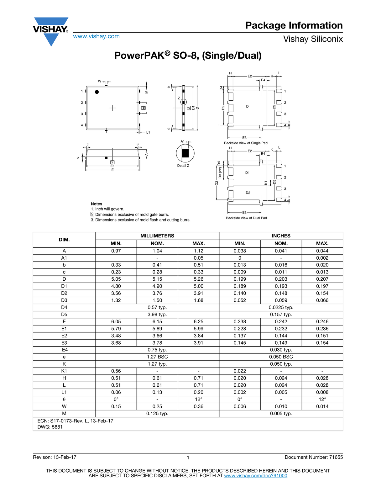
PowerPAK SO-8 Dimensions
Body: 5.05-5.26 mm (D) x 6.09-6.25 mm (E). Height: 0.97-1.12 mm (A). Lead pitch: 1.27 BSC mm. Exposed pad dimensions: 3.56-3.91 mm (D2) x 3.48-3.84 mm (E2).
Applications
- Synchronous rectification
- Primary side switching
- DC-DC converters
- OR-ing
- Power supplies
- Motor drive control
- Battery and load switch
Diagrams & Graphs (4)
## Description

The SiR680ADP is a high-performance N-channel 80 V power MOSFET from Vishay Siliconix in a PowerPAK SO-8 single package. Built on Vishay's TrenchFET Gen IV technology, it is optimized for the lowest RDS(on) x Qg and RDS(on) x Qoss figures of merit (FOM), making it ideal for synchronous rectification, primary-side switching, and DC-DC converter applications. The device delivers extremely low on-resistance (2.35 mOhm typical at VGS = 10 V) with a continuous drain current rating of 100 A at 25 C.

## Features

- TrenchFET Gen IV power MOSFET technology
- Very low RDS(on): 2.35 mOhm typ at VGS = 10 V, ID = 20 A
- Low RDS(on) x Qg figure of merit
- Tuned for lowest RDS(on) x Qoss FOM
- 100% Rg and UIS tested
- Continuous drain current: 100 A (at 25 C case temperature)
- Drain-source voltage: 80 V
- Gate-source voltage: +/- 20 V
- PowerPAK SO-8 package (leadless, exposed copper pad)
- RoHS compliant, halogen-free

## Pin Configuration

PowerPAK SO-8 Single configuration:

| Pin | Function |
|-----|----------|
| 1 | S (Source) |
| 2 | S (Source) |
| 3 | S (Source) |
| 4 | G (Gate) |
| 5 | D (Drain) |
| 6 | D (Drain) |
| 7 | D (Drain) |
| 8 | D (Drain) |
| Exposed pad | D (Drain) |

## Absolute Maximum Ratings

TA = 25 C unless otherwise noted.

| Parameter | Symbol | Limit | Unit |
|-----------|--------|-------|------|
| Drain-source voltage | VDS | 80 | V |
| Gate-source voltage | VGS | +/- 20 | V |
| Continuous drain current (TC = 25 C) | ID | 100 | A |
| Continuous drain current (TC = 70 C) | ID | 80.7 | A |
| Continuous drain current (TA = 25 C) | ID | 24.5 | A |
| Pulsed drain current (t <= 100 us) | IDM | 300 | A |
| Continuous source-drain diode current | IS | 5.6 | A |
| Single pulse avalanche current (L = 0.1 mH) | IAS | 80 | mJ |
| Single pulse avalanche energy | EAS | 104 | mJ |
| Maximum power dissipation (TC = 25 C) | PD | 125 | W |
| Maximum power dissipation (TC = 70 C) | PD | 68.6 | W |
| Maximum power dissipation (TA = 25 C) | PD | 6.25 | W |
| Maximum power dissipation (TA = 70 C) | PD | 4.1 | W |
| Operating junction and storage temperature | TJ, Tstg | -55 to +150 | C |
| Soldering recommendations (peak temperature) | - | 260 | C |

## Thermal Information

| Parameter | Symbol | Typical | Maximum | Unit |
|-----------|--------|---------|---------|------|
| Maximum junction-to-ambient (t <= 10 s) | RthJA | - | 20 | C/W |
| Maximum junction-to-case (drain) steady state | RthJC | 0.9 | 1.2 | C/W |

## Electrical Characteristics

TJ = 25 C unless otherwise noted.

### Static

| Parameter | Symbol | Test Conditions | Min | Typ | Max | Unit |
|-----------|--------|----------------|-----|-----|-----|------|
| Drain-source breakdown voltage | V(BR)DSS | VGS = 0 V, ID = 1 mA | 80 | -- | -- | V |
| VDS temperature coefficient | dV(BR)/dT | ID = 10 mA | -- | 61 | -- | mV/C |
| V(BR)DSS temperature coefficient | dV(BR)DSS/TJ | ID = 250 uA | -- | -8.2 | -- | mV/C |
| Gate-source threshold voltage | VGS(th) | VDS = VGS, ID = 250 uA | 2 | -- | 3.5 | V |
| Gate-source leakage | IGSS | VGS = +/- 20 V | -- | -- | 100 | nA |
| Zero gate voltage drain current | IDSS | VGS = 0 V | -- | -- | 1 | uA |
| On-state drain current | ID(on) | VGS = 10 V, VDS = 0.1 V | -- | 40 | -- | A |
| Drain-source on-resistance | RDS(on) | VGS = 10 V, ID = 20 A | -- | 0.00235 | 0.00288 | Ohm |
| Drain-source on-resistance | RDS(on) | VGS = 7.5 V, ID = 15 A | -- | 0.00270 | 0.00350 | Ohm |
| Forward transconductance | gfs | VDS = 15 V, ID = 20 A | -- | 68 | -- | S |

### Dynamic

| Parameter | Symbol | Test Conditions | Min | Typ | Max | Unit |
|-----------|--------|----------------|-----|-----|-----|------|
| Input capacitance | Ciss | VGS = 0 V, f = 1 MHz | -- | 4415 | -- | pF |
| Output capacitance | Coss | VDS = 40 V | -- | 614 | -- | pF |
| Reverse transfer capacitance | Crss | | -- | 26 | -- | pF |
| Total gate charge | Qg | VDS = 40 V, ID = 20 A | -- | 55 | 83 | nC |
| Gate-source charge | Qgs | VGS = 10 V | -- | 43 | 65 | nC |
| Gate-drain charge | Qgd | | -- | 17 | -- | nC |
| Gate resistance | Rg | f = 1 MHz | 0.3 | 0.88 | 1.5 | Ohm |
| Turn-on delay time | td(on) | VDD = 40 V, RL = 2 Ohm | -- | 17 | 34 | ns |
| Rise time | tr | ID = 20 A, RG = 1 Ohm | -- | 8 | 16 | ns |
| Turn-off delay time | td(off) | | -- | 30 | 60 | ns |
| Fall time | tf | | -- | 9 | 18 | ns |
| Turn-on delay time | td(on) | VDD = 40 V, RL = 2 Ohm | -- | 15 | 30 | ns |
| Rise time | tr | RG = 7.5 V, RG = 1 Ohm | -- | 9 | 18 | ns |
| Turn-off delay time | td(off) | | -- | 30 | 60 | ns |
| Fall time | tf | | -- | 9 | 18 | ns |

### Drain-Source Body Diode Characteristics

| Parameter | Symbol | Test Conditions | Min | Typ | Max | Unit |
|-----------|--------|----------------|-----|-----|-----|------|
| Continuous source-drain diode current | IS | TC = 25 C | -- | -- | 125 | A |
| Pulse diode forward current | ISM | | -- | -- | 300 | A |
| Body diode voltage | VSD | IS = 6 A, VGS = 0 V | -- | 0.72 | 1.1 | V |
| Body diode reverse recovery time | trr | | -- | 53 | 106 | ns |
| Body diode reverse recovery charge | Qrr | IF = 20 A, di/dt = 100 A/us | -- | 70 | 140 | nC |
| Reverse recovery fall time | ta | TJ = 25 C | -- | 30 | -- | ns |
| Reverse recovery rise time | tb | | -- | 23 | -- | ns |

## Packages

### Ordering Information

| Part Number | Package | Notes |
|-------------|---------|-------|
| SiR680ADP-T1-RE3 | PowerPAK SO-8 | Lead (Pb)-free and halogen-free |
| SiR680ADP-T1-GE3 | PowerPAK SO-8 | Lead (Pb)-free and halogen-free, BLR on ICL |
| SiR680ADP-T1-BE3 | PowerPAK SO-8 | Alternate manufacturing location |

### PowerPAK SO-8 Dimensions

Body: 5.05-5.26 mm (D) x 6.09-6.25 mm (E). Height: 0.97-1.12 mm (A). Lead pitch: 1.27 BSC mm. Exposed pad dimensions: 3.56-3.91 mm (D2) x 3.48-3.84 mm (E2).

## Applications

- Synchronous rectification
- Primary side switching
- DC-DC converters
- OR-ing
- Power supplies
- Motor drive control
- Battery and load switch
Sub-Skills
What are Sub-Skills?
Sub-skills are community-contributed AI skill extensions for this component.
They teach AI assistants about specific tools, configurators, or workflows.
Examples:
- A manufacturer’s configuration tool for a motor controller
- A community-written design guide for an amplifier circuit
- An automated test/validation script for a sensor module
How to add one: Click Add Sub-Skill, provide the URL
to your skill and a brief description. Submissions are reviewed by the Adom team
before going live.
Sub-skills are community-contributed AI skill extensions for this component. They teach AI assistants about specific tools, configurators, or workflows.
Examples:
- A manufacturer’s configuration tool for a motor controller
- A community-written design guide for an amplifier circuit
- An automated test/validation script for a sensor module
How to add one: Click Add Sub-Skill, provide the URL to your skill and a brief description. Submissions are reviewed by the Adom team before going live.
No sub-skills yet. Be the first to contribute one!