LM555 Timer
Texas Instruments LM555 timer/oscillator. 4.5–16V, 200mA output, 8-pin SOIC/PDIP/VSSOP. Standardized datasheet with 20 extracted diagrams, electrical characteristics, pin descriptions, and design charts.
Paste this into Claude Code (VS Code panel, Adom editor, or terminal) to install:
Search the Adom Wiki for the datasheet "LM555 Timer" (slug: lm555) at https://wiki-ufypy5dpx93o.adom.cloud/wiki/datasheets/lm555. Download the standardized markdown and extracted diagram images into my project's datasheets/lm555/ directory. Show me the key specifications and pin configuration.
Source: TI LM555 Datasheet (SNAS548D) Manufacturer: Texas Instruments Document: SNAS548D — Rev D, January 2015 Part Number: LM555
Description
The LM555 is a highly stable device for generating accurate time delays or oscillation. Additional terminals are provided for triggering or resetting if desired. In the time delay mode of operation, the time is precisely controlled by one external resistor and capacitor. For astable operation as an oscillator, the free running frequency and duty cycle are accurately controlled with two external resistors and one capacitor. The circuit may be triggered and reset on falling waveforms, and the output circuit can source or sink up to 200 mA or drive TTL circuits.
Key Specifications
Features
- • Direct replacement for SE555/NE555
- • Timing from microseconds through hours
- • Operates in both astable and monostable modes
- • Adjustable duty cycle
- • Output can source or sink 200 mA
- • Output and supply TTL compatible
- • Temperature stability better than 0.005% per °C
- • Normally on and normally off output
- • Available in 8-pin VSSOP package
Pin Configuration
Source: TI LM555 Datasheet (SNAS548D) Manufacturer: Texas Instruments Document: SNAS548D — Rev D, January 2015 Part Number: LM555
Absolute Maximum Ratings
| Parameter | Min | Max | Unit |
|---|---|---|---|
| Supply Voltage (VCC) | — | 18 | V |
| Power Dissipation — LM555CM/CN | — | 1180 | mW |
| Power Dissipation — LM555CMM (VSSOP) | — | 613 | mW |
| Storage Temperature | −65 | 150 | °C |
| ESD — Human Body Model (HBM) | — | ±500 | V |
Recommended Operating Conditions
| Parameter | Min | Max | Unit |
|---|---|---|---|
| Supply Voltage | 4.5 | 16 | V |
| Operating Temperature (TA) | 0 | 70 | °C |
Thermal Information
| Package | RθJA (°C/W) |
|---|---|
| PDIP-8 | 106 |
| SOIC-8 | 170 |
| VSSOP-8 | 204 |
Electrical Characteristics
TA = 25°C, VCC = 5V to 15V, unless otherwise specified.
| Parameter | Conditions | Min | Typ | Max | Unit |
|---|---|---|---|---|---|
| Supply Voltage | — | 4.5 | — | 16 | V |
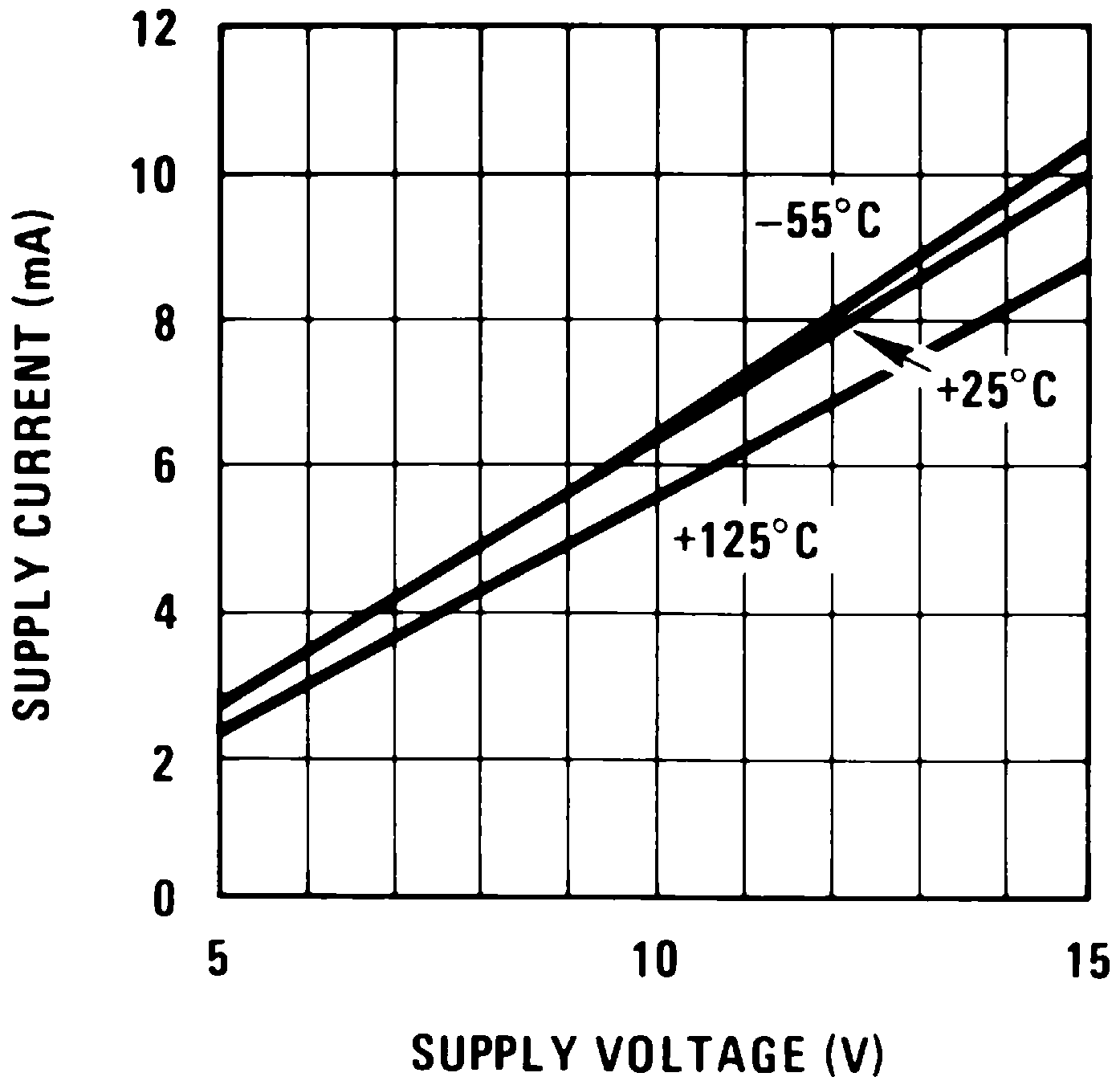
| Supply Current | VCC=5V, RL=∞ | — | 3 | 6 | mA |
| Supply Current | VCC=15V, RL=∞ | — | 10 | 15 | mA |
| Threshold Voltage | — | — | 0.667×VCC | — | V |
| Trigger Voltage | VCC=15V | — | 5 | — | V |
| Trigger Voltage | VCC=5V | — | 1.67 | — | V |
| Trigger Current | — | — | 0.5 | 0.9 | µA |
| Reset Voltage | — | — | 0.5 | 1 | V |
| Reset Current | — | — | 0.1 | 0.4 | mA |
| Threshold Current | — | — | 0.1 | 0.25 | µA |
| Control Voltage | VCC=15V | 9 | 10 | 11 | V |
| Control Voltage | VCC=5V | 2.6 | 3.33 | 4 | V |
| Pin 7 Leakage (High) | — | — | 1 | 100 | nA |
| Pin 7 Saturation | VCC=15V, I7=15mA | — | — | 180 | mV |
| Output Low (VOL) | ISINK=10mA | — | 0.1 | 0.25 | V |
| Output Low (VOL) | ISINK=50mA | — | 0.4 | 0.75 | V |
| Output Low (VOL) | ISINK=100mA | — | 2 | 2.5 | V |
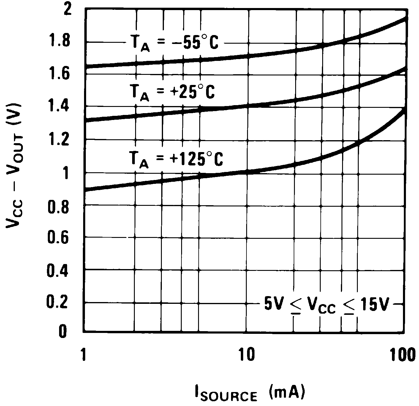
| Output High (VOH) | ISRC=100mA, VCC=15V | 12.75 | — | 13.3 | V |
| Output High (VOH) | ISRC=100mA, VCC=5V | 2.75 | — | 3.3 | V |
| Rise Time | — | — | 100 | — | ns |
| Fall Time | — | — | 100 | — | ns |
Timing Accuracy
| Parameter | Mode | Value | Unit |
|---|---|---|---|
| Initial Accuracy | Monostable | 1% | — |
| Drift with Temperature | Monostable | 50 | ppm/°C |
| Accuracy over Temperature | Monostable | 1.5% | — |
| Drift with Supply | Monostable | 0.1% | /V |
| Initial Accuracy | Astable | 2.25% | — |
| Drift with Temperature | Astable | 150 | ppm/°C |
| Accuracy over Temperature | Astable | 3% | — |
| Drift with Supply | Astable | 0.30% | /V |
Packages
| Package | Body Size | RθJA |
|---|---|---|
| SOIC-8 (LM555CM) | 4.90 × 3.91 mm | 170 °C/W |
| PDIP-8 (LM555CN) | 9.81 × 6.35 mm | 106 °C/W |
| VSSOP-8 (LM555CMM) | 3.00 × 3.00 mm | 204 °C/W |
Applications
- Precision Timing
- Pulse Generation
- Sequential Timing
- Time Delay Generation
- Pulse Width Modulation (PWM)
- Pulse Position Modulation
- Linear Ramp Generator
Key Formulas
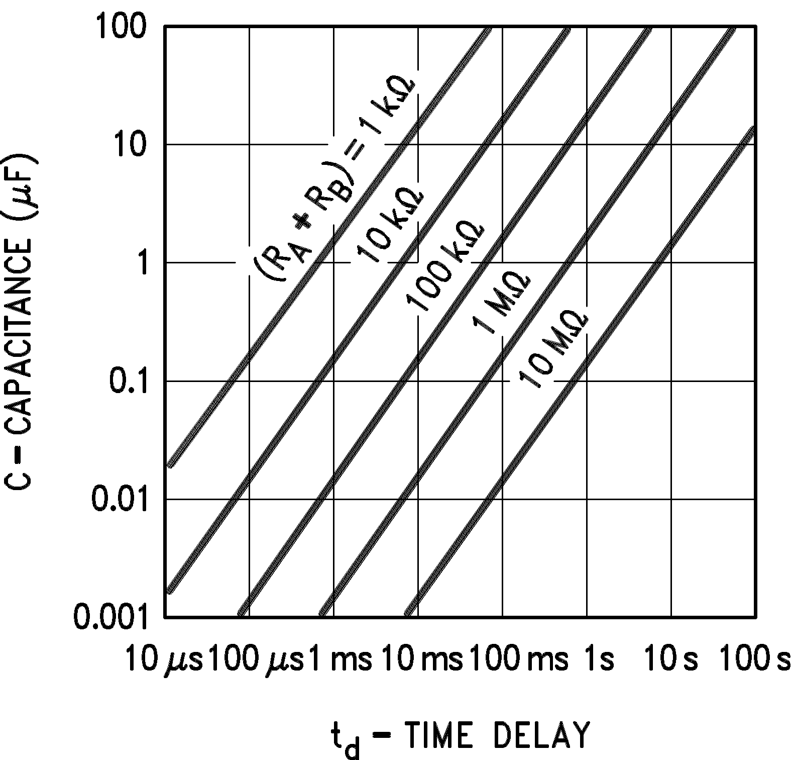
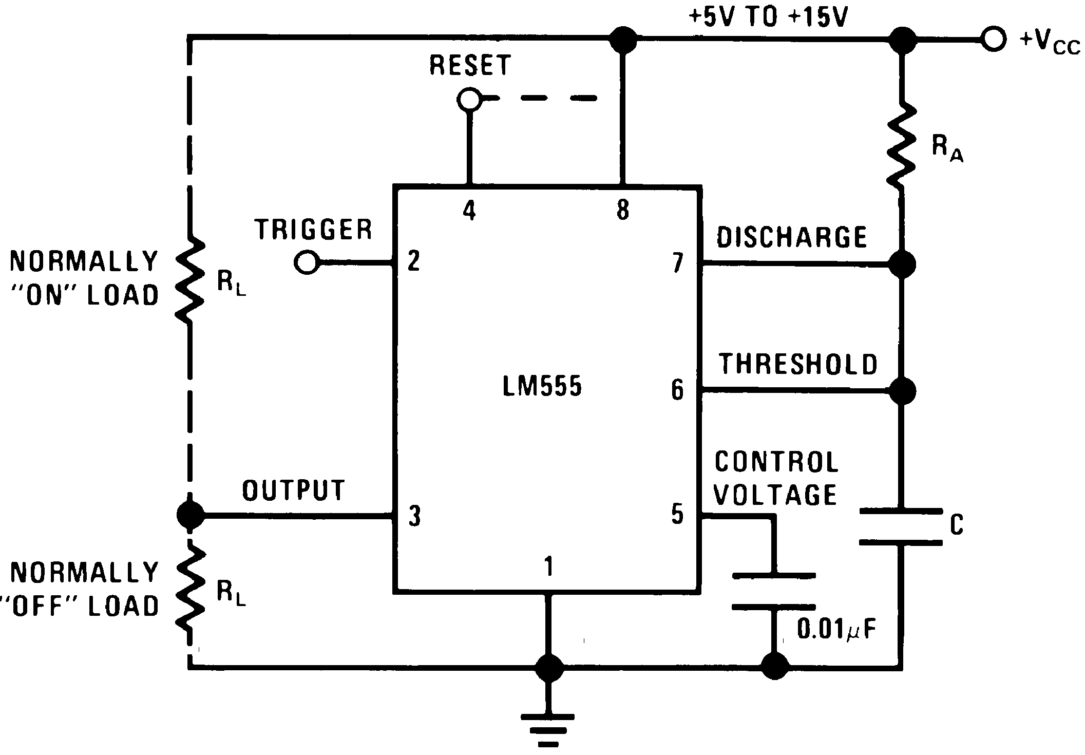
Monostable (One-Shot) — Time Delay: t = 1.1 × RA × C
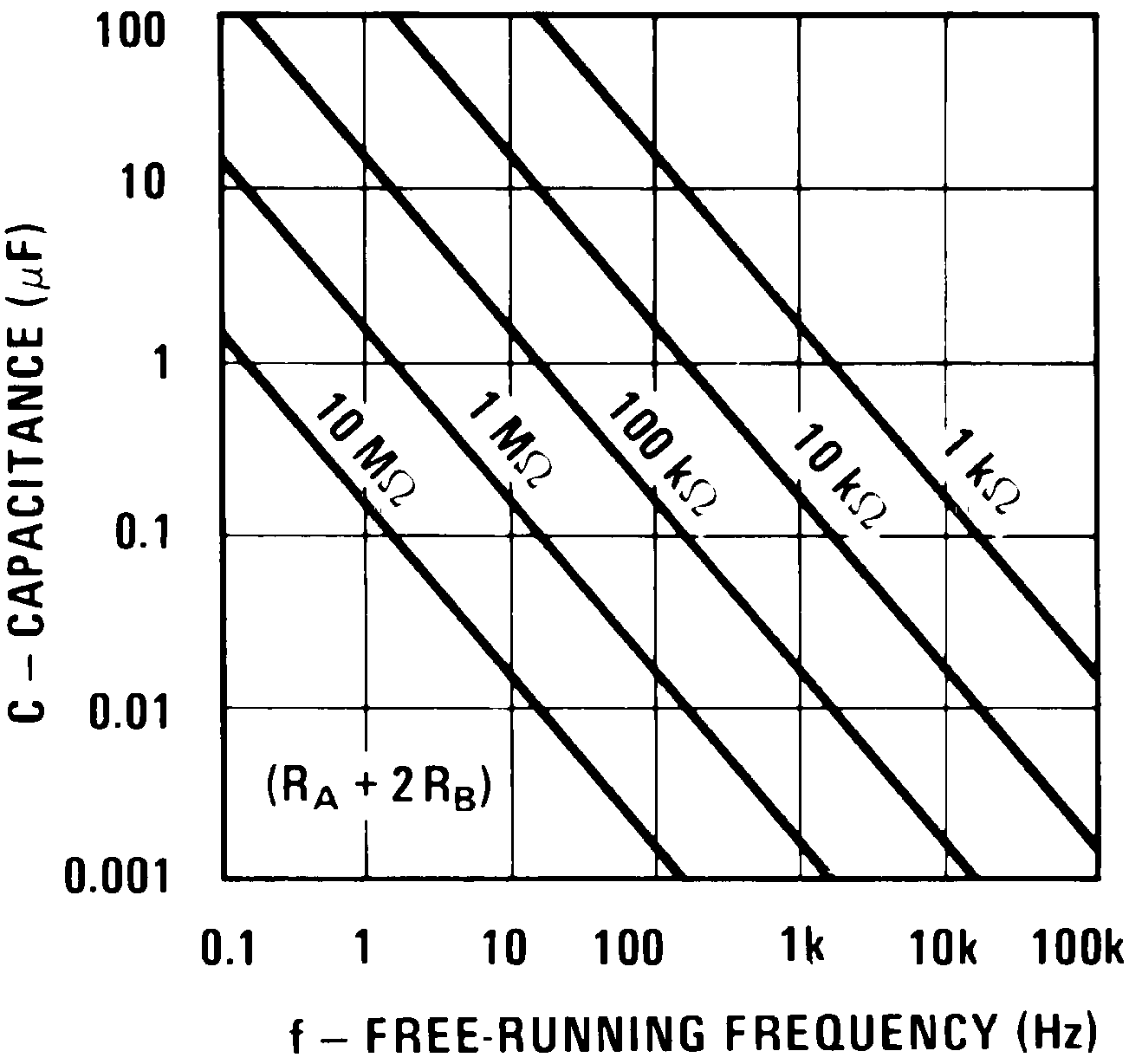
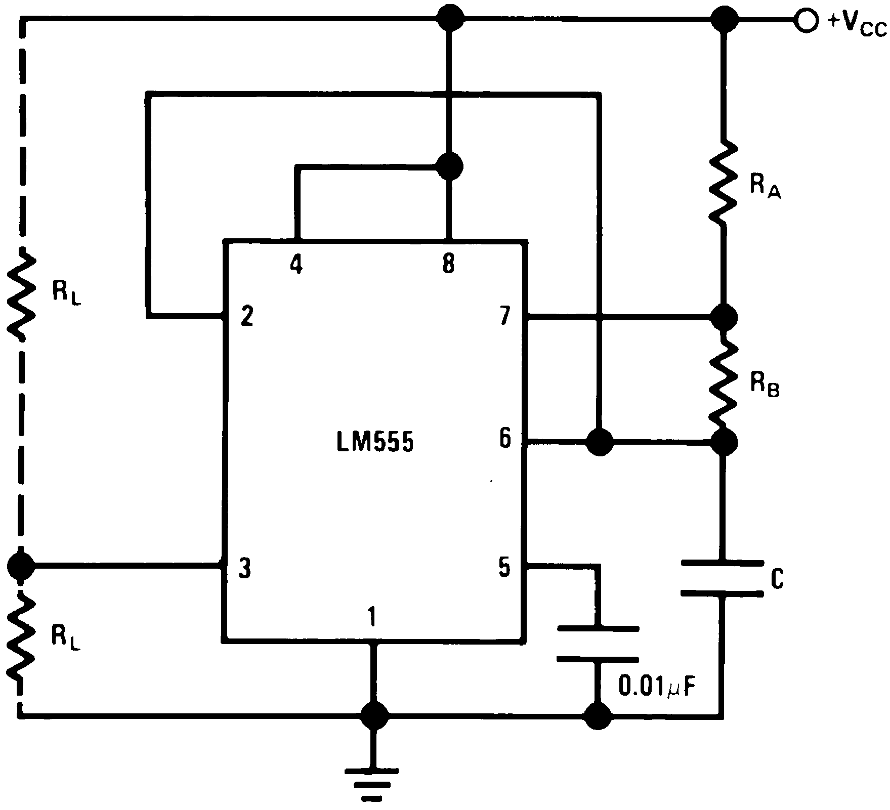
Astable — Frequency: f = 1.44 / ((RA + 2·RB) × C)
Astable — Duty Cycle: D = (RA + RB) / (RA + 2·RB)
Conditions: RA = 1kΩ to 100kΩ, C = 0.1µF. Maximum total RA + RB = 20MΩ for 15V operation.
Diagrams & Graphs (8)
# LM555 Timer — Parsed Datasheet

**Source:** [TI LM555 Datasheet (SNAS548D)](https://www.ti.com/lit/ds/symlink/lm555.pdf)
**Manufacturer:** Texas Instruments
**Document:** SNAS548D — Rev D, January 2015
**Part Number:** LM555

## Description

The LM555 is a highly stable device for generating accurate time delays or oscillation. Additional terminals are provided for triggering or resetting if desired. In the time delay mode of operation, the time is precisely controlled by one external resistor and capacitor. For astable operation as an oscillator, the free running frequency and duty cycle are accurately controlled with two external resistors and one capacitor. The circuit may be triggered and reset on falling waveforms, and the output circuit can source or sink up to 200 mA or drive TTL circuits.

## Key Specifications

| Parameter | Value |
|-----------|-------|
| Supply Voltage | 4.5V – 16V |
| Output Current | 200 mA (source or sink) |
| Pin Count | 8 |
| Supply Current | 3–15 mA |
| Temperature Stability | 0.005%/°C |
| Rise / Fall Time | 100 ns |
| ESD Rating (HBM) | ±500V |

## Features

- Direct replacement for SE555/NE555
- Timing from microseconds through hours
- Operates in both astable and monostable modes
- Adjustable duty cycle
- Output can source or sink 200 mA
- Output and supply TTL compatible
- Temperature stability better than 0.005% per °C
- Normally on and normally off output
- Available in 8-pin VSSOP package

## Pin Configuration

| Pin | Name | Direction | Description |
|-----|------|-----------|-------------|
| 1 | GND | GND | Ground reference voltage (0V) |
| 2 | TRIGGER | IN | Triggers on voltage falling below 1/3 VCC. Responsible for flip-flop set-to-reset transition. |
| 3 | OUTPUT | OUT | Output driven waveform. Can source or sink up to 200 mA. TTL compatible. |
| 4 | RESET | IN | Active low reset. Connect to VCC when not used to avoid false triggering. Threshold 0.4–1V. |
| 5 | CONTROL VOLTAGE | IN | Controls threshold/trigger levels. Determines pulse width. Typically bypassed with 10nF to GND. |
| 6 | THRESHOLD | IN | Compares applied voltage with 2/3 VCC reference. Sets the internal flip-flop. Input current 0.1–0.25 µA. |
| 7 | DISCHARGE | IN | Open collector output. Discharges timing capacitor between intervals. |
| 8 | VCC | PWR | Positive supply voltage 4.5V to 16V. Bypass with 100nF ceramic. |

## Absolute Maximum Ratings

| Parameter | Min | Max | Unit |
|-----------|-----|-----|------|
| Supply Voltage (VCC) | — | 18 | V |
| Power Dissipation — LM555CM/CN | — | 1180 | mW |
| Power Dissipation — LM555CMM (VSSOP) | — | 613 | mW |
| Storage Temperature | −65 | 150 | °C |
| ESD — Human Body Model (HBM) | — | ±500 | V |

## Recommended Operating Conditions

| Parameter | Min | Max | Unit |
|-----------|-----|-----|------|
| Supply Voltage | 4.5 | 16 | V |
| Operating Temperature (TA) | 0 | 70 | °C |

## Thermal Information

| Package | RθJA (°C/W) |
|---------|-------------|
| PDIP-8 | 106 |
| SOIC-8 | 170 |
| VSSOP-8 | 204 |

## Electrical Characteristics

TA = 25°C, VCC = 5V to 15V, unless otherwise specified.

| Parameter | Conditions | Min | Typ | Max | Unit |
|-----------|-----------|-----|-----|-----|------|
| Supply Voltage | — | 4.5 | — | 16 | V |
| Supply Current | VCC=5V, RL=∞ | — | 3 | 6 | mA |
| Supply Current | VCC=15V, RL=∞ | — | 10 | 15 | mA |
| Threshold Voltage | — | — | 0.667×VCC | — | V |
| Trigger Voltage | VCC=15V | — | 5 | — | V |
| Trigger Voltage | VCC=5V | — | 1.67 | — | V |
| Trigger Current | — | — | 0.5 | 0.9 | µA |
| Reset Voltage | — | — | 0.5 | 1 | V |
| Reset Current | — | — | 0.1 | 0.4 | mA |
| Threshold Current | — | — | 0.1 | 0.25 | µA |
| Control Voltage | VCC=15V | 9 | 10 | 11 | V |
| Control Voltage | VCC=5V | 2.6 | 3.33 | 4 | V |
| Pin 7 Leakage (High) | — | — | 1 | 100 | nA |
| Pin 7 Saturation | VCC=15V, I7=15mA | — | — | 180 | mV |
| Output Low (VOL) | ISINK=10mA | — | 0.1 | 0.25 | V |
| Output Low (VOL) | ISINK=50mA | — | 0.4 | 0.75 | V |
| Output Low (VOL) | ISINK=100mA | — | 2 | 2.5 | V |
| Output High (VOH) | ISRC=100mA, VCC=15V | 12.75 | — | 13.3 | V |
| Output High (VOH) | ISRC=100mA, VCC=5V | 2.75 | — | 3.3 | V |
| Rise Time | — | — | 100 | — | ns |
| Fall Time | — | — | 100 | — | ns |

## Timing Accuracy

| Parameter | Mode | Value | Unit |
|-----------|------|-------|------|
| Initial Accuracy | Monostable | 1% | — |
| Drift with Temperature | Monostable | 50 | ppm/°C |
| Accuracy over Temperature | Monostable | 1.5% | — |
| Drift with Supply | Monostable | 0.1% | /V |
| Initial Accuracy | Astable | 2.25% | — |
| Drift with Temperature | Astable | 150 | ppm/°C |
| Accuracy over Temperature | Astable | 3% | — |
| Drift with Supply | Astable | 0.30% | /V |

## Packages

| Package | Body Size | RθJA |
|---------|-----------|------|
| SOIC-8 (LM555CM) | 4.90 × 3.91 mm | 170 °C/W |
| PDIP-8 (LM555CN) | 9.81 × 6.35 mm | 106 °C/W |
| VSSOP-8 (LM555CMM) | 3.00 × 3.00 mm | 204 °C/W |

## Applications

- Precision Timing
- Pulse Generation
- Sequential Timing
- Time Delay Generation
- Pulse Width Modulation (PWM)
- Pulse Position Modulation
- Linear Ramp Generator

## Key Formulas

**Monostable (One-Shot) — Time Delay:**
`t = 1.1 × RA × C`

**Astable — Frequency:**
`f = 1.44 / ((RA + 2·RB) × C)`

**Astable — Duty Cycle:**
`D = (RA + RB) / (RA + 2·RB)`

Conditions: RA = 1kΩ to 100kΩ, C = 0.1µF. Maximum total RA + RB = 20MΩ for 15V operation.

## Diagrams

20 figures extracted from the datasheet PDF. See attached image assets.

### Circuit Diagrams
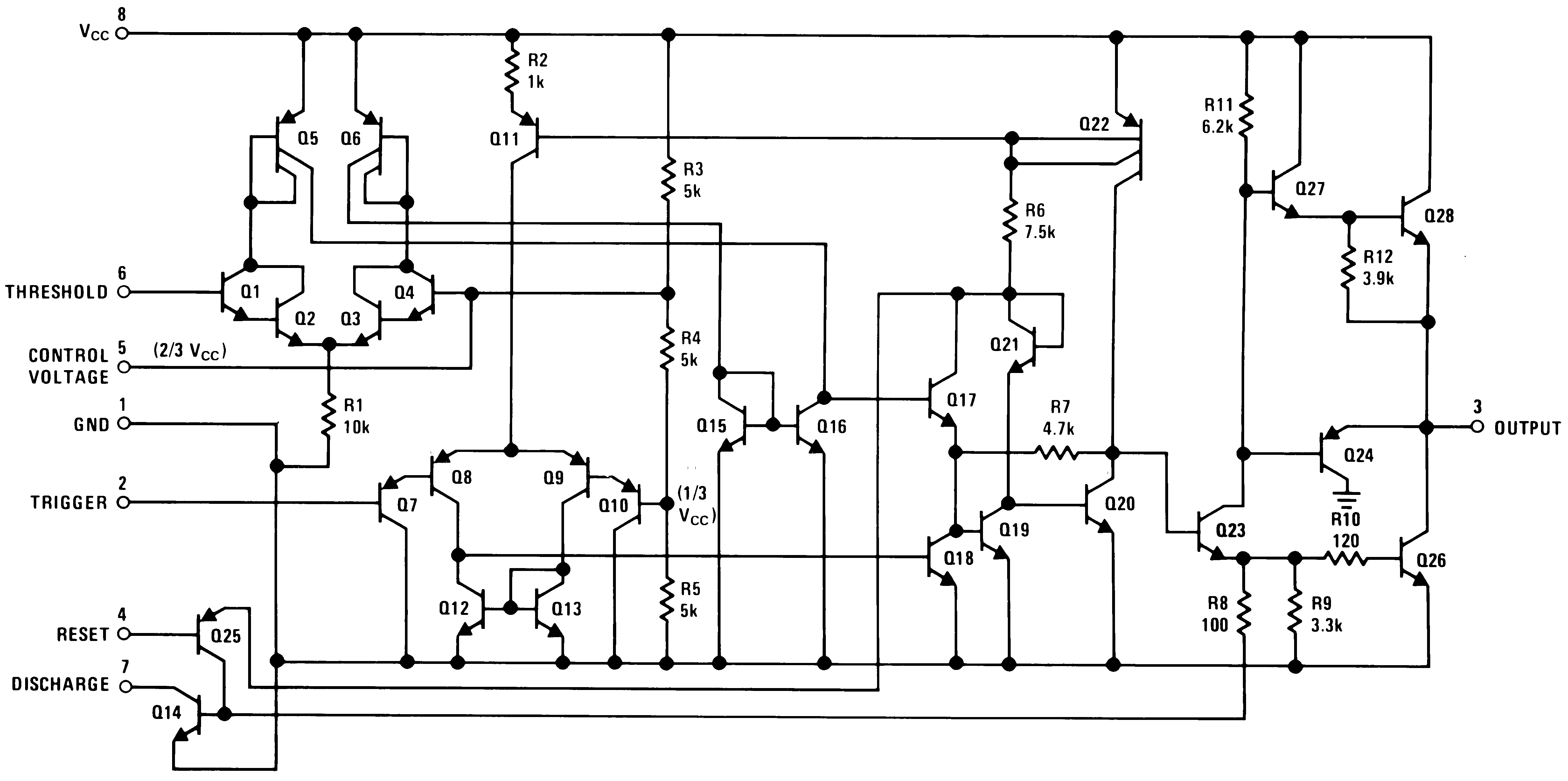
- `schematic-internal.png` — Complete transistor-level schematic (28 transistors, 12 resistors)
- `circuit-monostable.png` — Monostable (one-shot) application circuit
- `circuit-astable.png` — Astable (oscillator) application circuit
- `circuit-monostable-example.png` — Practical monostable with pushbutton + LED

### Electrical Characteristics
- `char-supply-current-vs-voltage.png` — ICC vs VCC across temperature
- `char-vout-high-drop-vs-isource.png` — Output high voltage drop vs source current
- `char-vout-low-vs-isink-5v.png` — Output low voltage at VCC=5V
- `char-vout-low-vs-isink-10v.png` — Output low voltage at VCC=10V
- `char-vout-low-vs-isink-15v.png` — Output low voltage at VCC=15V
- `char-min-trigger-pulse.png` — Minimum trigger pulse width
- `char-discharge-vsat-15v.png` — Pin 7 saturation voltage at VCC=15V
- `char-discharge-vsat-5v.png` — Pin 7 saturation voltage at VCC=5V
- `char-prop-delay-multi-vcc.png` — Propagation delay vs trigger (multi-VCC)
- `char-prop-delay-multi-temp.png` — Propagation delay vs trigger (multi-temperature)

### Waveforms
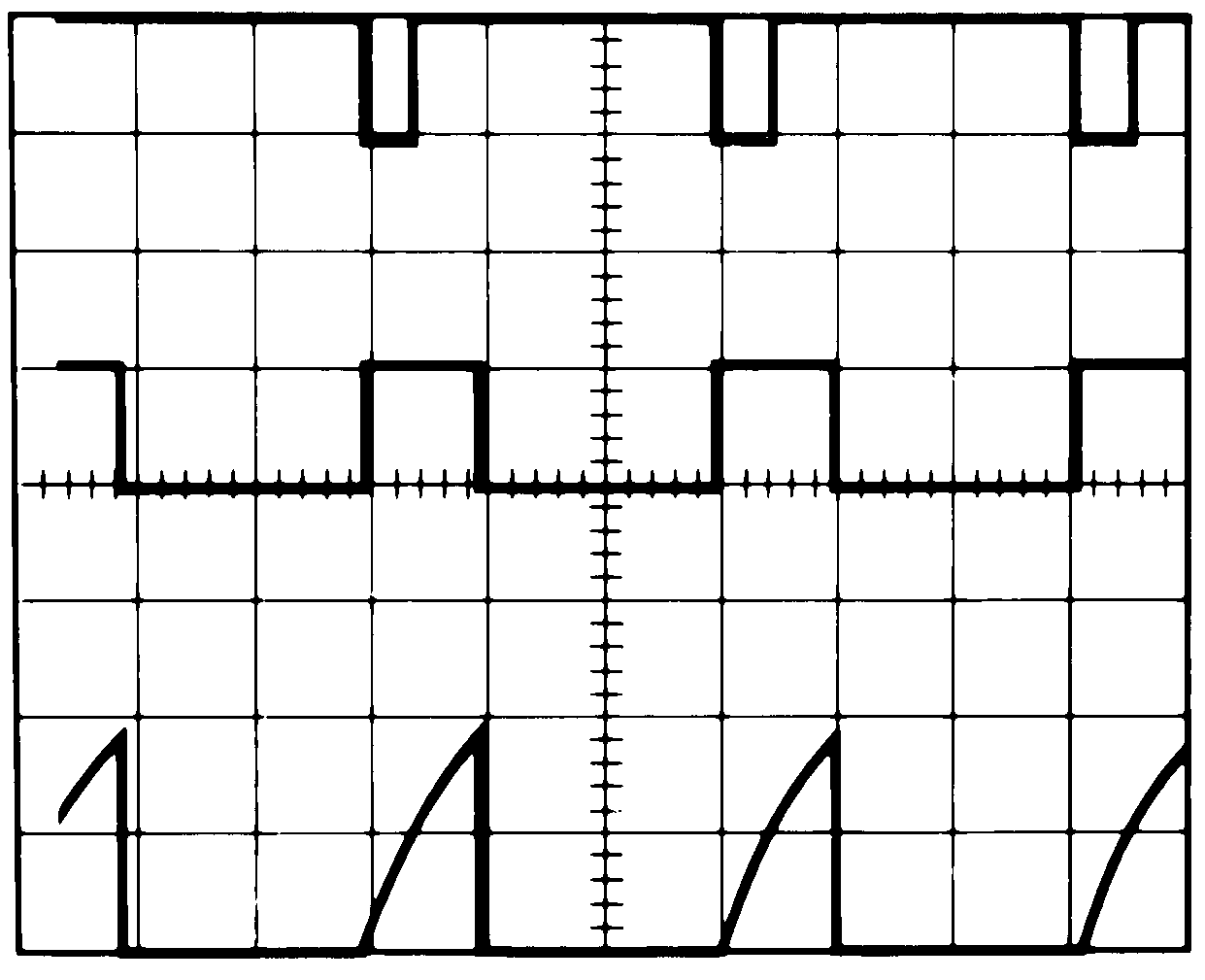
- `waveform-astable-3ch.png` — Astable mode: output + trigger + capacitor
- `waveform-astable-2ch.png` — Astable mode: output + capacitor sawtooth
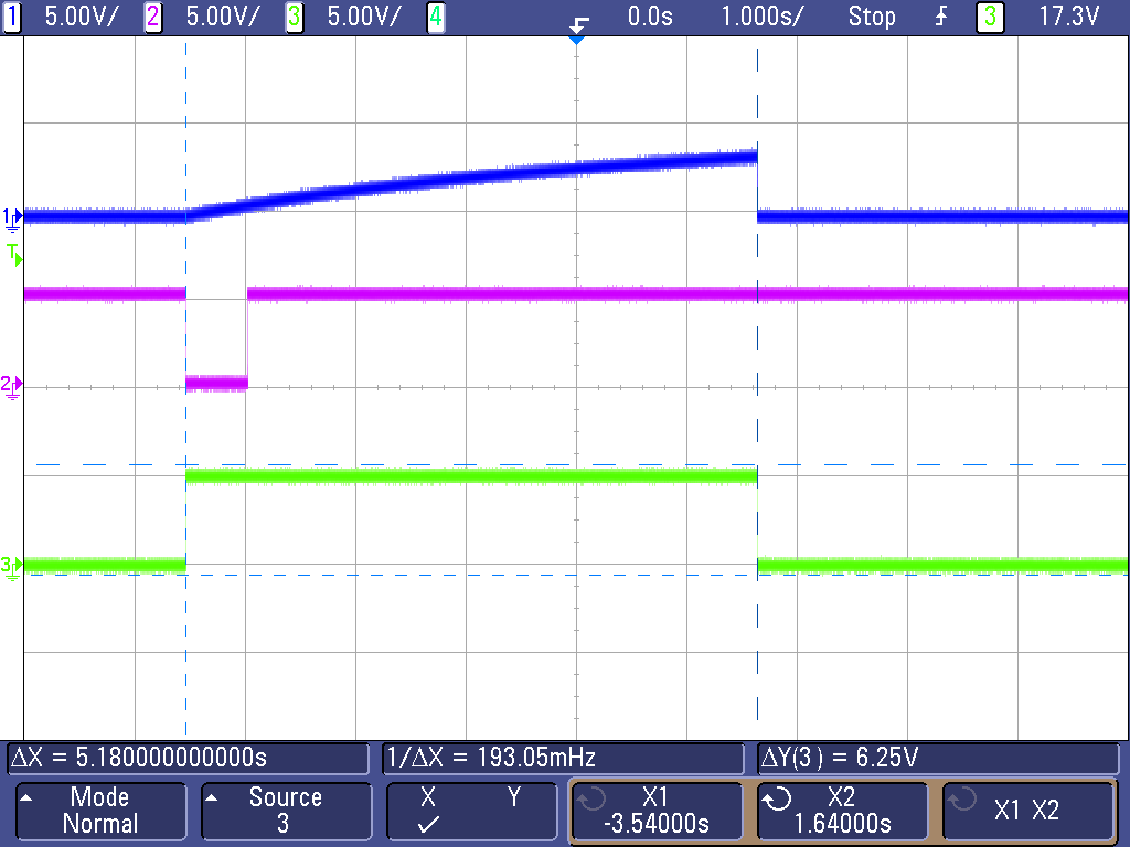
- `waveform-monostable.png` — Monostable mode: output + reset + capacitor
- `waveform-oscilloscope-color.png` — Real oscilloscope capture (3-channel, color)

### Design Charts
- `chart-monostable-time-delay.png` — Capacitance vs time delay nomograph
- `chart-astable-frequency.png` — Capacitance vs frequency nomograph
Sub-Skills
What are Sub-Skills?
Sub-skills are community-contributed AI skill extensions for this component.
They teach AI assistants about specific tools, configurators, or workflows.
Examples:
- A manufacturer’s configuration tool for a motor controller
- A community-written design guide for an amplifier circuit
- An automated test/validation script for a sensor module
How to add one: Click Add Sub-Skill, provide the URL
to your skill and a brief description. Submissions are reviewed by the Adom team
before going live.
Sub-skills are community-contributed AI skill extensions for this component. They teach AI assistants about specific tools, configurators, or workflows.
Examples:
- A manufacturer’s configuration tool for a motor controller
- A community-written design guide for an amplifier circuit
- An automated test/validation script for a sensor module
How to add one: Click Add Sub-Skill, provide the URL to your skill and a brief description. Submissions are reviewed by the Adom team before going live.
No sub-skills yet. Be the first to contribute one!