BMM350 — 3-Axis High-Performance Magnetometer
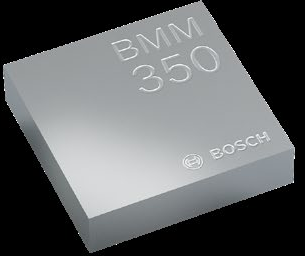
Bosch Sensortec BMM350. TMR-based 3-axis magnetometer, +/-2000 uT range, 190 nT noise, I2C/I3C, 1.28x1.28mm WLCSP. Standardized datasheet with 14 extracted diagrams.
Paste this into Claude Code (VS Code panel, Adom editor, or terminal) to install:
Search the Adom Wiki for the datasheet "BMM350 — 3-Axis High-Performance Magnetometer" (slug: bmm350) at https://wiki-ufypy5dpx93o.adom.cloud/wiki/datasheets/bmm350. Download the standardized markdown and extracted diagram images into my project's datasheets/bmm350/ directory. Show me the key specifications and pin configuration.
Source: Bosch Sensortec Datasheet (BST-BMM350-DS001-27) Manufacturer: Bosch Sensortec Part Number: BMM350 Document: BST-BMM350-DS001-27 — Rev 1.27, February 2025
Description
The BMM350 is a high-performance 3-axis geomagnetic sensor based on Bosch Sensortec's proprietary TMR (tunnel magnetoresistance) technology. It measures magnetic field strength in three perpendicular axes and is designed for demanding consumer applications such as electronic compass, tilt-compensated navigation, augmented/virtual/mixed reality, image stabilization, indoor navigation, dead-reckoning, and robotics.
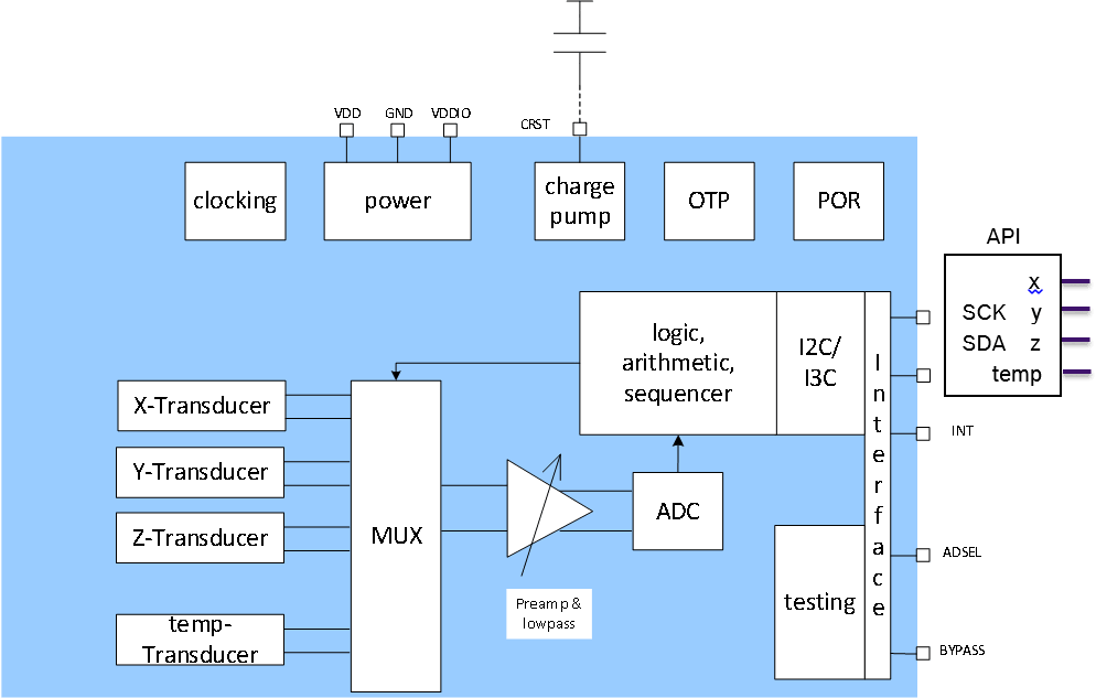
An evaluation ASIC converts the TMR transducer output to 21-bit digital results accessible over I2C or I3C interfaces. Each device is factory-calibrated and compensated via an on-chip OTP and a host-side API. The BMM350 features an excellent temperature behavior with outstanding low temperature coefficients of offset (TCO) and sensitivity (TCS). The ultra-small WLCSP package (1.28 x 1.28 x 0.5 mm) makes it ideal for space-constrained mobile and wearable designs.
Key Specifications
Features
- • 3-axis magnetic field sensing based on proprietary TMR technology
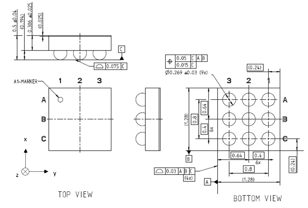
- • Ultra-small WLCSP package: 1.28 x 1.28 x 0.5 mm (9-ball, 0.4 mm pitch)
- • Digital interfaces: I2C (standard/fast/fast+) and I3C (SDR, 12.5 MHz) with in-band interrupt
- • Wide VDDIO range from 1.72V to 3.6V for flexible system integration
- • Ultra-low power: 200 uA typical at 100 Hz ODR (regular power preset)
- • Four noise/power presets: Low Power, Regular Power, Low Noise, Ultra Low Noise
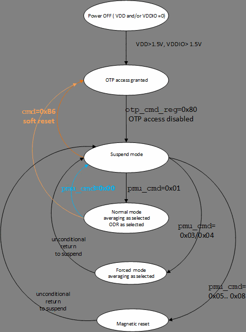
- • Normal mode (periodic) and forced mode (triggered, single-shot) operation
- • On-chip interrupt controller with configurable polarity, drive type, and latching
- • Automatic magnetic reset for recovery from excessive field exposure
- • Built-in self-test for X and Y axis verification
- • 24-bit sensortime counter with 40 us resolution
- • Factory-calibrated with OTP compensation coefficients
- • Comprehensive C API for rapid host integration
- • I2C watchdog for communication fault recovery
- • RoHS compliant and halogen-free
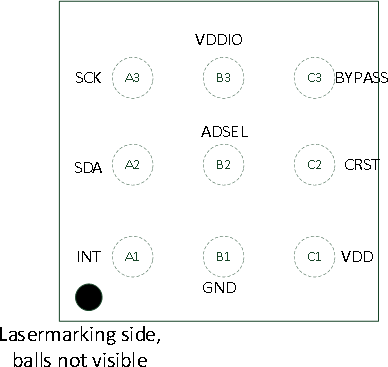
Pin Configuration
Source: Bosch Sensortec Datasheet (BST-BMM350-DS001-27) Manufacturer: Bosch Sensortec Part Number: BMM350 Document: BST-BMM350-DS001-27 — Rev 1.27, February 2025
Absolute Maximum Ratings
| Parameter | Condition | Min | Max | Unit |
|---|---|---|---|---|
| VDD Pin Voltage | — | -0.3 | 2 | V |
| VDDIO Pin Voltage | — | -0.3 | 3.6 | V |
| Non-Supply Pin Voltage | — | -0.3 | VDDIO + 0.3 | V |
| Operating Temperature | Active operation | -40 | +85 | C |
| Storage Temperature | <=65% rel. humidity | -50 | +125 | C |
| OTP Data Retention | T = 85 C | — | 10 | years |
| Mechanical Shock | Duration <=500 us | — | 20,000 | g |
| ESD (HBM) | Any pin | — | +/-2 | kV |
| ESD (CDM) | — | — | +/-500 | V |
| Latch-up | — | — | +/-100 | mA |
| Magnetic Field | Any direction | -250 | 250 | mT |
Electrical Characteristics
| Parameter | Condition | Min | Typ | Max | Unit |
|---|---|---|---|---|---|
| Supply Voltage VDD | — | 1.72 | — | 1.98 | V |
| Supply Voltage VDDIO | — | 1.72 | — | 3.6 | V |
| Input Low Voltage | I2C/I3C | — | — | 0.3 VDDIO | V |
| Input High Voltage | I2C/I3C | 0.7 VDDIO | — | — | V |
| Output Low Voltage | IOL <= 2 mA | — | — | 0.23 VDDIO | V |
| Output High Voltage | IOH <= 2 mA | 0.8 VDDIO | — | — | V |
| Magnetic Field Range | All axes | -2000 | — | +2000 | uT |
| Zero-Field Offset Drift | Before/after solder | — | — | +/-25 | uT |
| Zero-B Offset (calibrated) | With eCompass SW, RT | — | — | +/-2 | uT |
| Sensitivity Error (X/Y) | After API compensation, RT | — | +/-1 | — | % |
| Sensitivity Error (Z) | After API compensation, RT | — | +/-3 | — | % |
| Sensitivity Temp Drift (TCS) | -40 to +85 C, all axes | — | +/-0.010 | — | %/K |
| TCO Error | -40 to +85 C | — | — | +/-200 | nT/K |
| Hysteresis (X/Y) | RT, after FSS | — | 0.02 | — | %FS |
| Hysteresis (Z) | RT, after FSS, no reset | — | 0.4 | — | %FS |
| Integral Nonlinearity (X/Y) | Deviation from best-fit line | — | — | +/-10 | uT |
| Integral Nonlinearity (Z) | Deviation from best-fit line | — | — | +/-20 | uT |
| Output Noise RMS (X/Y) | ODR=100, avg=2 | — | 190 | — | nT(rms) |
| Output Noise RMS (Z) | ODR=100, avg=2 | — | 450 | — | nT(rms) |
| ODR Drift over Temp | -5 to 65 C | -3 | — | +3 | % |
| ODR Drift over Temp | -40 to 85 C | -4 | — | +4 | % |
| 3 dB Bandwidth | — | — | ODR/2 | — | Hz |
| Startup Time (Suspend to Normal) | — | — | 70 | — | ms |
| Startup Time (OFF to Suspend) | — | — | 2.5 | — | ms |
| Peak Supply Current | Measurement phase, before bit reset | — | 3.5 | — | mA |
Power Consumption
| Noise Mode | Averaging | ODR 400 Hz | ODR 200 Hz | ODR 100 Hz | ODR 50 Hz | ODR 25 Hz | ODR 12.5 Hz |
|---|---|---|---|---|---|---|---|
| Ultra Low Noise | 8 samples (avg=3) | — | — | — | 325 uA | 180 uA | 108 uA |
| Low Noise | 4 samples (avg=2) | — | — | 335 uA | 175 uA | 96 uA | 57 uA |
| Regular Power | 2 samples (avg=1) | — | 370 uA | 190 uA | 100 uA | 55 uA | 33 uA |
| Low Power | 1 sample (avg=0) | 455 uA | 235 uA | 122 uA | 70 uA | 40 uA | 23 uA |
| Suspend Mode | — | — | — | 1.8 uA | — | — | — |
Forced mode maximum trigger rates: avg=1: 200 Hz, avg=2: 150 Hz, avg=4: 80 Hz, avg=8: 40 Hz.
Communication Interface
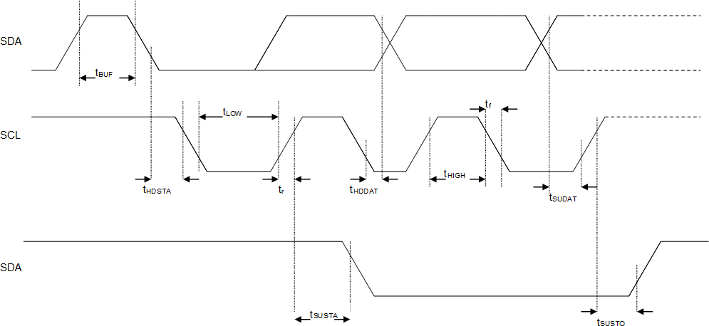
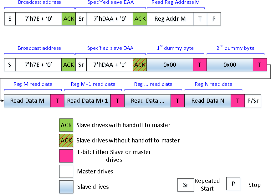
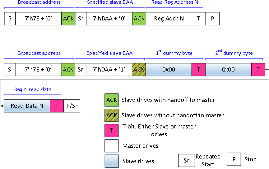
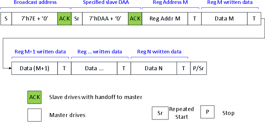
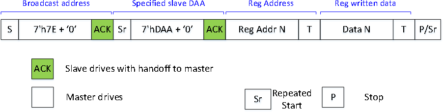
The BMM350 supports I2C (standard, fast, fast+ modes) and I3C (SDR up to 12.5 MHz) digital interfaces. The sensor acts as a slave device on both protocols.
I2C Address: 7-bit address is 0x14 (ADSEL=LOW) or 0x15 (ADSEL=HIGH). The 5 MSBs are fixed (00101); bit 1 is OTP-backed (default 0); bit 0 is set by the ADSEL pin level at boot.
I2C Features:
- Single and multiple byte write (register address + data pairs, not auto-incremented)
- Single and multiple byte read (auto-incremented addresses)
- 2 dummy bytes prepended to every read (must be discarded)
- Configurable watchdog: short timeout (1.28 ms) or long timeout (40.96 ms)
I3C Features:
- SDR mode up to 12.5 MHz clock
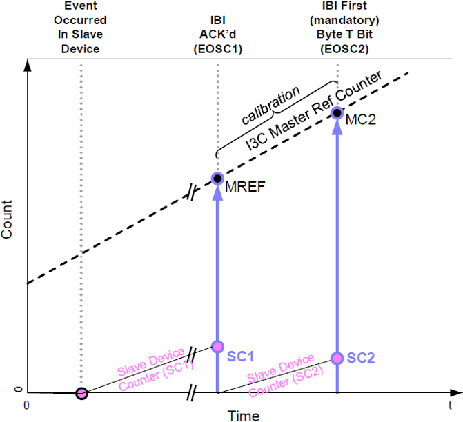
- In-band interrupt (IBI) for data-ready signaling
- Timing control asynchronous mode 0 (4.32 MHz internal slave clock)
- Provisional ID: MIPI Member ID 0x03b8, Part ID includes CHIP_ID (0x33)
- Supported CCCs: ENEC, DISEC, RSTDAA, ENTDAA, SETAASA, SETDASA, SETNEWDA, RSTACT, SETXTIME, GETXTIME, GETPID, GETBCR, GETDCR, GETSTATUS, GETCAPS
Interrupt Configuration:
- Data-ready interrupt mapped to INT pin (configurable)
- Polarity: active-high or active-low
- Drive type: push-pull or open-drain
- Latching or non-latching (pulsed, 1.25 ms auto-clear)
- I3C in-band interrupt with optional auto-clear of status
Packages
| Package | Pins | Body Size | Ball Pitch | Height |
|---|---|---|---|---|
| WLCSP | 9 | 1.28 mm x 1.28 mm | 0.4 mm | 0.5 mm |
External Components Required:
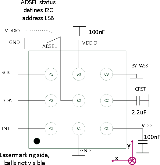
- 100 nF decoupling capacitor on VDD to GND
- 100 nF decoupling capacitor on VDDIO to GND
- 2.2 uF low-inductance, low-ESR capacitor on CRST (recommended: TDK CGB4B3X7R0J225K055AB)
PCB Design Notes:
- Reserve 1.3 x 1.3 mm footprint area for the IC
- Peak current up to 400 mA (< 1 us) between CRST capacitor and CRST/GND pins
- VDD pin: 20 mA max short-term, 750 uA max average
- ADSEL pin must not be left floating
- CRST capacitor must have non-magnetic properties
Software API
The BMM350 is supported by Bosch Sensortec's official C API available at github.com/boschsensortec/BMM350_SensorAPI.
Key API Functions:
BMM350_init()— Initialize sensor, download OTP compensation data, terminate boot phaseBMM350_set_powermode()— Switch between suspend, normal, and forced modesBMM350_set_odr_performance()— Configure output data rate and noise/averaging presetBMM350_read_mag_data_and_compensate()— Read raw data and apply full compensation (offset, gain, temperature)BMM350_check_for_highfield_and_reset()— Detect excessive field and trigger magnetic resetBMM350_magnetic_reset_and_wait()— Perform manual magnetic reset (for suspend-mode recovery)BMM350_perform_self_test()— Run built-in self-test on X and Y channelsBMM350_enable_interrupt()/BMM350_configure_interrupt()— Set up data-ready interruptBMM350_set_int_ctrl_ibi()— Configure I3C in-band interruptBMM350_enable_axes()— Enable/disable individual measurement axesBMM350_set_pad_drive()— Configure pad driver strength (0=weakest to 7=strongest)BMM350_set_i2c_wdt()— Enable/configure I2C watchdogBMM350_set_ctrl_user()— Enable sensortime always-on modeBMM350_soft_reset_and_wait()— Trigger soft reset (CMD = 0xB6 then 0x00)
Register Map: 8-bit register space from 0x00 to 0x7E. Key registers include CHIP_ID (0x00, value 0x33), PMU_CMD (0x06), data registers (0x31-0x3F for X/Y/Z magnetic + temperature + sensortime), INT_CTRL (0x2E), and CMD (0x7E).
Data Format: Magnetic and temperature data are provided in 24-bit registers using 21-bit signed integer format. Burst read is mandatory to ensure data consistency (the sensor halts register updates during burst reads).
Applications
- Magnetic heading information and electronic compass
- Tilt-compensated map rotation and navigation
- Augmented reality (AR), virtual reality (VR), and mixed reality (MR)
- Gyroscope calibration in 9-DoF IMU systems
- Indoor navigation and dead-reckoning (e.g., step counting with accelerometer)
- Platform and image stabilization
- Robotics navigation
- High-end gaming controllers
- Man-machine interfaces
Key Formulas
Excessive Field Limit
SQRT(Hx^2 + Hy^2 + Hz^2) <= 2000 uTThe sum of the vector components must remain within the 2000 uT sphere.
Self-Test Threshold
delta_x = mag_x(during_selftest) - mag_x(before_selftest) >= 130 uT
delta_y = mag_y(during_selftest) - mag_y(before_selftest) >= 130 uT
Sensortime Resolution
sensortime_seconds = sensortime_register_value * 40e-624-bit unsigned counter, wraps around at 2^24 (no saturation). Resolution is 40 us per tick.
I2C Address Calculation
I2C_address = 0b0010_10X (7-bit)
X = ADSEL pin level at boot
ADSEL=LOW  -> 0x14
ADSEL=HIGH -> 0x15
Noise Improvement with Averaging
noise_rms_improved = noise_rms_single / SQRT(averaging_samples)
averaging_samples = 2^avg  (avg = 0,1,2,3 -> 1,2,4,8 samples)
Diagrams & Graphs (14)


**Source:** [Bosch Sensortec Datasheet (BST-BMM350-DS001-27)](https://www.bosch-sensortec.com/media/boschsensortec/downloads/datasheets/bst-bmm350-ds001.pdf)
**Manufacturer:** Bosch Sensortec
**Part Number:** BMM350
**Document:** BST-BMM350-DS001-27 — Rev 1.27, February 2025

## Description

The BMM350 is a high-performance 3-axis geomagnetic sensor based on Bosch Sensortec's proprietary TMR (tunnel magnetoresistance) technology. It measures magnetic field strength in three perpendicular axes and is designed for demanding consumer applications such as electronic compass, tilt-compensated navigation, augmented/virtual/mixed reality, image stabilization, indoor navigation, dead-reckoning, and robotics.

An evaluation ASIC converts the TMR transducer output to 21-bit digital results accessible over I2C or I3C interfaces. Each device is factory-calibrated and compensated via an on-chip OTP and a host-side API. The BMM350 features an excellent temperature behavior with outstanding low temperature coefficients of offset (TCO) and sensitivity (TCS). The ultra-small WLCSP package (1.28 x 1.28 x 0.5 mm) makes it ideal for space-constrained mobile and wearable designs.

## Key Specifications

| Parameter | Value |
| --- | --- |
| Magnetic Field Range | +/-2000 uT (all axes) |
| Field Resolution | ~0.1 uT |
| Output Noise (X/Y, RMS) | 190 nT @ ODR=100 Hz, avg=2 |
| Output Noise (Z, RMS) | 450 nT @ ODR=100 Hz, avg=2 |
| Supply Voltage (VDD) | 1.72V to 1.98V |
| I/O Supply Voltage (VDDIO) | 1.72V to 3.6V |
| Current (Normal, 100 Hz) | 200 uA typical (regular power) |
| Current (Suspend) | 1.8 uA typical |
| Output Data Rates | 1.5625 Hz to 400 Hz |
| Data Resolution | 21-bit signed integer |
| Digital Interface | I2C (up to Fast+ mode), I3C (SDR up to 12.5 MHz) |
| Operating Temperature | -40 C to +85 C |
| Package | WLCSP 9-ball, 1.28 x 1.28 x 0.5 mm |
| Pin Count | 9 |

## Features

- 3-axis magnetic field sensing based on proprietary TMR technology
- Ultra-small WLCSP package: 1.28 x 1.28 x 0.5 mm (9-ball, 0.4 mm pitch)
- Digital interfaces: I2C (standard/fast/fast+) and I3C (SDR, 12.5 MHz) with in-band interrupt
- Wide VDDIO range from 1.72V to 3.6V for flexible system integration
- Ultra-low power: 200 uA typical at 100 Hz ODR (regular power preset)
- Four noise/power presets: Low Power, Regular Power, Low Noise, Ultra Low Noise
- Normal mode (periodic) and forced mode (triggered, single-shot) operation
- On-chip interrupt controller with configurable polarity, drive type, and latching
- Automatic magnetic reset for recovery from excessive field exposure
- Built-in self-test for X and Y axis verification
- 24-bit sensortime counter with 40 us resolution
- Factory-calibrated with OTP compensation coefficients
- Comprehensive C API for rapid host integration
- I2C watchdog for communication fault recovery
- RoHS compliant and halogen-free

## Pin Configuration

| Pin | Name | Type | Description |
| --- | --- | --- | --- |
| C1 | VDD | Power | Digital and analog supply (1.72V to 1.98V), use 100 nF decoupling capacitor |
| B3 | VDDIO | Power | I/O supply (1.72V to 3.6V), use 100 nF decoupling capacitor |
| B1 | GND | Power | Analog, digital and I/O ground |
| A3 | SCK | Digital | I2C / I3C serial clock (SCL) |
| A2 | SDA | Digital | I2C / I3C serial data (SDA) |
| A1 | INT | Output | Interrupt output (push-pull or open-drain, configurable polarity) |
| B2 | ADSEL | Input | I2C address LSB select; connect to GND (0x14) or VDDIO (0x15) |
| C2 | CRST | Analog | External 2.2 uF capacitor for magnetic reset (low-inductance, low-ESR) |
| C3 | BYPASS | Power | Connect to ground |

## Absolute Maximum Ratings

| Parameter | Condition | Min | Max | Unit |
| --- | --- | --- | --- | --- |
| VDD Pin Voltage | — | -0.3 | 2 | V |
| VDDIO Pin Voltage | — | -0.3 | 3.6 | V |
| Non-Supply Pin Voltage | — | -0.3 | VDDIO + 0.3 | V |
| Operating Temperature | Active operation | -40 | +85 | C |
| Storage Temperature | <=65% rel. humidity | -50 | +125 | C |
| OTP Data Retention | T = 85 C | — | 10 | years |
| Mechanical Shock | Duration <=500 us | — | 20,000 | g |
| ESD (HBM) | Any pin | — | +/-2 | kV |
| ESD (CDM) | — | — | +/-500 | V |
| Latch-up | — | — | +/-100 | mA |
| Magnetic Field | Any direction | -250 | 250 | mT |

## Electrical Characteristics

| Parameter | Condition | Min | Typ | Max | Unit |
| --- | --- | --- | --- | --- | --- |
| Supply Voltage VDD | — | 1.72 | — | 1.98 | V |
| Supply Voltage VDDIO | — | 1.72 | — | 3.6 | V |
| Input Low Voltage | I2C/I3C | — | — | 0.3 VDDIO | V |
| Input High Voltage | I2C/I3C | 0.7 VDDIO | — | — | V |
| Output Low Voltage | IOL <= 2 mA | — | — | 0.23 VDDIO | V |
| Output High Voltage | IOH <= 2 mA | 0.8 VDDIO | — | — | V |
| Magnetic Field Range | All axes | -2000 | — | +2000 | uT |
| Zero-Field Offset Drift | Before/after solder | — | — | +/-25 | uT |
| Zero-B Offset (calibrated) | With eCompass SW, RT | — | — | +/-2 | uT |
| Sensitivity Error (X/Y) | After API compensation, RT | — | +/-1 | — | % |
| Sensitivity Error (Z) | After API compensation, RT | — | +/-3 | — | % |
| Sensitivity Temp Drift (TCS) | -40 to +85 C, all axes | — | +/-0.010 | — | %/K |
| TCO Error | -40 to +85 C | — | — | +/-200 | nT/K |
| Hysteresis (X/Y) | RT, after FSS | — | 0.02 | — | %FS |
| Hysteresis (Z) | RT, after FSS, no reset | — | 0.4 | — | %FS |
| Integral Nonlinearity (X/Y) | Deviation from best-fit line | — | — | +/-10 | uT |
| Integral Nonlinearity (Z) | Deviation from best-fit line | — | — | +/-20 | uT |
| Output Noise RMS (X/Y) | ODR=100, avg=2 | — | 190 | — | nT(rms) |
| Output Noise RMS (Z) | ODR=100, avg=2 | — | 450 | — | nT(rms) |
| ODR Drift over Temp | -5 to 65 C | -3 | — | +3 | % |
| ODR Drift over Temp | -40 to 85 C | -4 | — | +4 | % |
| 3 dB Bandwidth | — | — | ODR/2 | — | Hz |
| Startup Time (Suspend to Normal) | — | — | 70 | — | ms |
| Startup Time (OFF to Suspend) | — | — | 2.5 | — | ms |
| Peak Supply Current | Measurement phase, before bit reset | — | 3.5 | — | mA |

## Power Consumption

| Noise Mode | Averaging | ODR 400 Hz | ODR 200 Hz | ODR 100 Hz | ODR 50 Hz | ODR 25 Hz | ODR 12.5 Hz |
| --- | --- | --- | --- | --- | --- | --- | --- |
| Ultra Low Noise | 8 samples (avg=3) | — | — | — | 325 uA | 180 uA | 108 uA |
| Low Noise | 4 samples (avg=2) | — | — | 335 uA | 175 uA | 96 uA | 57 uA |
| Regular Power | 2 samples (avg=1) | — | 370 uA | 190 uA | 100 uA | 55 uA | 33 uA |
| Low Power | 1 sample (avg=0) | 455 uA | 235 uA | 122 uA | 70 uA | 40 uA | 23 uA |
| Suspend Mode | — | — | — | 1.8 uA | — | — | — |

Forced mode maximum trigger rates: avg=1: 200 Hz, avg=2: 150 Hz, avg=4: 80 Hz, avg=8: 40 Hz.

## Communication Interface

The BMM350 supports **I2C** (standard, fast, fast+ modes) and **I3C** (SDR up to 12.5 MHz) digital interfaces. The sensor acts as a slave device on both protocols.

**I2C Address:** 7-bit address is 0x14 (ADSEL=LOW) or 0x15 (ADSEL=HIGH). The 5 MSBs are fixed (00101); bit 1 is OTP-backed (default 0); bit 0 is set by the ADSEL pin level at boot.

**I2C Features:**
- Single and multiple byte write (register address + data pairs, not auto-incremented)
- Single and multiple byte read (auto-incremented addresses)
- 2 dummy bytes prepended to every read (must be discarded)
- Configurable watchdog: short timeout (1.28 ms) or long timeout (40.96 ms)

**I3C Features:**
- SDR mode up to 12.5 MHz clock
- In-band interrupt (IBI) for data-ready signaling
- Timing control asynchronous mode 0 (4.32 MHz internal slave clock)
- Provisional ID: MIPI Member ID 0x03b8, Part ID includes CHIP_ID (0x33)
- Supported CCCs: ENEC, DISEC, RSTDAA, ENTDAA, SETAASA, SETDASA, SETNEWDA, RSTACT, SETXTIME, GETXTIME, GETPID, GETBCR, GETDCR, GETSTATUS, GETCAPS

**Interrupt Configuration:**
- Data-ready interrupt mapped to INT pin (configurable)
- Polarity: active-high or active-low
- Drive type: push-pull or open-drain
- Latching or non-latching (pulsed, 1.25 ms auto-clear)
- I3C in-band interrupt with optional auto-clear of status

## Packages

| Package | Pins | Body Size | Ball Pitch | Height |
| --- | --- | --- | --- | --- |
| WLCSP | 9 | 1.28 mm x 1.28 mm | 0.4 mm | 0.5 mm |

**External Components Required:**
- 100 nF decoupling capacitor on VDD to GND
- 100 nF decoupling capacitor on VDDIO to GND
- 2.2 uF low-inductance, low-ESR capacitor on CRST (recommended: TDK CGB4B3X7R0J225K055AB)

**PCB Design Notes:**
- Reserve 1.3 x 1.3 mm footprint area for the IC
- Peak current up to 400 mA (< 1 us) between CRST capacitor and CRST/GND pins
- VDD pin: 20 mA max short-term, 750 uA max average
- ADSEL pin must not be left floating
- CRST capacitor must have non-magnetic properties

## Software API

The BMM350 is supported by Bosch Sensortec's official C API available at [github.com/boschsensortec/BMM350_SensorAPI](https://github.com/boschsensortec/BMM350_SensorAPI/blob/main/README.md).

**Key API Functions:**
- `BMM350_init()` — Initialize sensor, download OTP compensation data, terminate boot phase
- `BMM350_set_powermode()` — Switch between suspend, normal, and forced modes
- `BMM350_set_odr_performance()` — Configure output data rate and noise/averaging preset
- `BMM350_read_mag_data_and_compensate()` — Read raw data and apply full compensation (offset, gain, temperature)
- `BMM350_check_for_highfield_and_reset()` — Detect excessive field and trigger magnetic reset
- `BMM350_magnetic_reset_and_wait()` — Perform manual magnetic reset (for suspend-mode recovery)
- `BMM350_perform_self_test()` — Run built-in self-test on X and Y channels
- `BMM350_enable_interrupt()` / `BMM350_configure_interrupt()` — Set up data-ready interrupt
- `BMM350_set_int_ctrl_ibi()` — Configure I3C in-band interrupt
- `BMM350_enable_axes()` — Enable/disable individual measurement axes
- `BMM350_set_pad_drive()` — Configure pad driver strength (0=weakest to 7=strongest)
- `BMM350_set_i2c_wdt()` — Enable/configure I2C watchdog
- `BMM350_set_ctrl_user()` — Enable sensortime always-on mode
- `BMM350_soft_reset_and_wait()` — Trigger soft reset (CMD = 0xB6 then 0x00)

**Register Map:** 8-bit register space from 0x00 to 0x7E. Key registers include CHIP_ID (0x00, value 0x33), PMU_CMD (0x06), data registers (0x31-0x3F for X/Y/Z magnetic + temperature + sensortime), INT_CTRL (0x2E), and CMD (0x7E).

**Data Format:** Magnetic and temperature data are provided in 24-bit registers using 21-bit signed integer format. Burst read is mandatory to ensure data consistency (the sensor halts register updates during burst reads).

## Applications

- Magnetic heading information and electronic compass
- Tilt-compensated map rotation and navigation
- Augmented reality (AR), virtual reality (VR), and mixed reality (MR)
- Gyroscope calibration in 9-DoF IMU systems
- Indoor navigation and dead-reckoning (e.g., step counting with accelerometer)
- Platform and image stabilization
- Robotics navigation
- High-end gaming controllers
- Man-machine interfaces

## Key Formulas

### Excessive Field Limit
```
SQRT(Hx^2 + Hy^2 + Hz^2) <= 2000 uT
```
The sum of the vector components must remain within the 2000 uT sphere.

### Self-Test Threshold
```
delta_x = mag_x(during_selftest) - mag_x(before_selftest) >= 130 uT
delta_y = mag_y(during_selftest) - mag_y(before_selftest) >= 130 uT
```

### Sensortime Resolution
```
sensortime_seconds = sensortime_register_value * 40e-6
```
24-bit unsigned counter, wraps around at 2^24 (no saturation). Resolution is 40 us per tick.

### I2C Address Calculation
```
I2C_address = 0b0010_10X (7-bit)
X = ADSEL pin level at boot
ADSEL=LOW  -> 0x14
ADSEL=HIGH -> 0x15
```

### Noise Improvement with Averaging
```
noise_rms_improved = noise_rms_single / SQRT(averaging_samples)
averaging_samples = 2^avg  (avg = 0,1,2,3 -> 1,2,4,8 samples)
```
Sub-Skills
What are Sub-Skills?
Sub-skills are community-contributed AI skill extensions for this component.
They teach AI assistants about specific tools, configurators, or workflows.
Examples:
- A manufacturer’s configuration tool for a motor controller
- A community-written design guide for an amplifier circuit
- An automated test/validation script for a sensor module
How to add one: Click Add Sub-Skill, provide the URL
to your skill and a brief description. Submissions are reviewed by the Adom team
before going live.
Sub-skills are community-contributed AI skill extensions for this component. They teach AI assistants about specific tools, configurators, or workflows.
Examples:
- A manufacturer’s configuration tool for a motor controller
- A community-written design guide for an amplifier circuit
- An automated test/validation script for a sensor module
How to add one: Click Add Sub-Skill, provide the URL to your skill and a brief description. Submissions are reviewed by the Adom team before going live.
No sub-skills yet. Be the first to contribute one!